In the previous tutorial, the basic combinational arithmetic circuits like half adder, full adder, half subtractor and full subtractor were discussed in details. Now, in this tutorial, the truth table and derivation of the boolean expressions for all those circuits will be considered. With the derived boolean expressions, all those circuits will be practically designed using digital ICs.
As discussed in the previous tutorial, the half adder can be constructed using an EX-OR gate and the AND gate. The full adder can be constructed using an OR gate, two EX-OR gates and two AND gates. The half subtractor can be constructed using an EX-OR gate, a NOT gate and an AND gate. The full subtractor can be constructed with an OR gate, two EX-OR gates, two AND gates and two NOT gates. So, for testing all the circuits, two AND gates, two EX-OR gates, two NOT gates and an OR gate are required. For AND gate, 7408 IC can be used which has four AND Gates in-built. For OR gate, 7432 IC can be used which has four OR gates in-built. For EX-OR gate, 7486 IC can be used which has four EX-OR gates in-built. For NOT gate, 7404 IC can be used which has six NOT gates in-built. The input to the digital circuits built from these ICs can be given from a DC supply of 2V while the supply voltage to the ICs can be given from a DC supply of 5V. The 5V DC supply can be constructed using a battery and 7805 IC. The same voltage can be dropped for inputs using a variable resistor. The output can be checked by connecting LEDs at the respective digital output pins.
So, Let us start testing the basic combinational circuits with digital ICs mentioned above.
Circuit Diagrams –
The Half adder has the following circuit diagram –

Fig. 1: Circuit Diagram of Half Adder
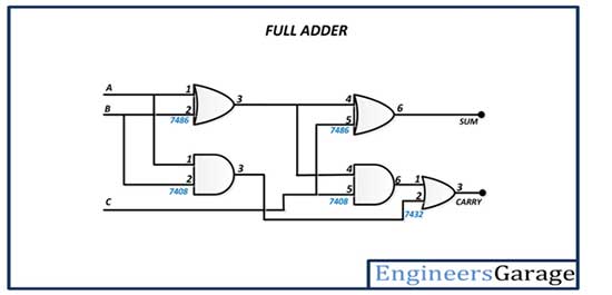
The Full Adder has the following circuit diagram –

Fig. 2: Circuit Diagram of Full Adder
The half subtractor has the following circuit diagram –

Fig. 3: Circuit Diagram of Half Subtractor
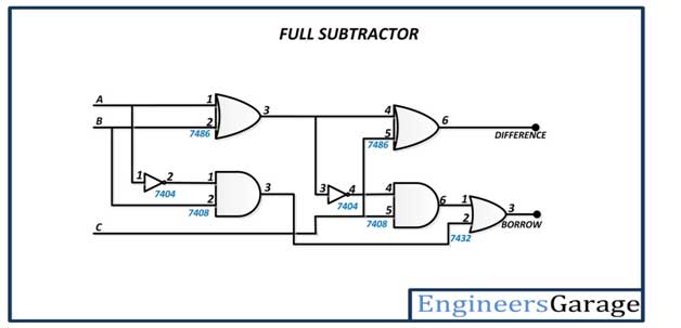
The full subtractor has the following circuit diagram –

Fig. 4: Circuit Diagram of Full Subtractor
Circuit Connections –
All the combinational arithmetic circuits are built by interconnecting the logic gates. Each combinational circuit has its own unique truth table where each output is linked to the inputs by some boolean function. The circuits are built by interconnecting the logic gate ICs. The following logic gate ICs are used in the construction of the circuits –
7408 IC – The 7408 IC has quad 2-input AND gates. The IC has the following pin configuration –

Fig. 5: Table listing pin configuration of 7408 IC
The IC has the following Pin Diagram –

Fig. 6: Pin Diagram of 7408 IC
The IC requires a supply voltage of 5V which can be tolerated up to 7V. The voltage at the inputs of AND gates must be 2V for high logic and 0V for low logic. The output of the AND gates has a voltage of 3.4 V for high logic and 0.2 V for low logic. The IC operates on positive logic system. The propagation delay while transiting from LOW to HIGH level at the output is 27 ns while propagation delay while transiting from HIGH to LOW level at the output is 19 ns.
7432 IC – The 7432 IC has quad 2-input OR gates. The IC has the following pin configuration –

Fig. 7: Table listing pin configuration of 7432 IC
The IC has the following Pin Diagram –
Fig. 7: Pin Diagram of 7432 IC
The IC requires a supply voltage of 5V which can be tolerated up to 7V. The voltage at the inputs of OR gates must be 2V for high logic and 0V for low logic. The output of the OR gates has a voltage of 3.4 V for high logic and 0.35 V for low logic. The IC operates on positive logic system. The propagation delay while transiting from LOW to HIGH level at the output comes 3 to 15 ns while propagation delay while transiting from HIGH to LOW level at the output also comes 3 to 15 ns.
7486 IC – The 7486 IC has quad 2-input EX-OR gates. The IC has the following pin configuration –

Fig. 8: Table listing pin configuration of 7486 IC
The IC has the following Pin Diagram –

Fig. 9: Pin Diagram of 7486 IC
The IC requires a supply voltage of 5V which can be tolerated up to 7V. The voltage at the inputs of EX-OR gates must be 2V for high logic and 0V for low logic. The output of the EX-OR gates has a voltage of 3.4 V for high logic and 0.2 V for low logic. The IC operates on positive logic system. The propagation delay while transiting from LOW to HIGH level at the output is 23 ns if other inputs are low and 30 ns if other inputs are high while propagation delay while transiting from HIGH to LOW level at the output is 17 ns if other inputs are low and 22 ns if other inputs are high.
7404 IC – The 7404 IC has six inverting gates. The IC has the following pin configuration –

Fig. 10: Table listing pin configuration of 7404 IC
The IC has the following Pin Diagram –

Fig. 11: Pin Diagram of 7404 IC
The IC requires a supply voltage of 5V which can be tolerated up to 7V. The voltage at the inputs of NOT gates must be 2V for high logic and 0.8 V for low logic. The output of the NOT gates have a voltage of 3.4 V for high logic and 0.2 V for low logic. The IC operates on positive logic system. The propagation delay while transiting from LOW to HIGH level at the output is 22 ns while propagation delay while transiting from HIGH to LOW level at the output is 15 ns.
It must be noted that the selected ICs have compatible input, output and supply voltage levels. They are taken from a common family (74XX series) of digital ICs.
The half adder is constructed by connecting the inputs to an EX-OR gate (pins 1 and 2 of 7486 IC) and an AND gate (pins 1 and 2 of 7408 IC). The Sum bit is drawn from output of the EX-OR gate (pin 3 of 7486 IC) and the carry is drawn from output of the AND gate (pin 3 of 7408 IC).
The full adder is constructed by connecting the inputs to one EX-OR gate (pins 1 and 2 of 7486 IC) and one AND gate (pins 1 and 2 of 7408 IC). The output from first EX-OR gate (pin 3 of 7486 IC) is connected to input of second EX-OR gate (pin 4 of 7486 IC) and input of second AND gate (pin 4 of 7408 IC). The Carry input is connected to another input of the second EX-OR gate (pin 5 of 7486 IC) and other input of second AND gate (pin 5 of 7408 IC). The sum bit is drawn from output of the second EX-OR gate (pin 6 of 7486 IC). The output from second AND gate (pin 6 of 7408 IC) is connected to one input of OR gate (pin 1 of 7432 IC) and output from first AND gate (pin 3 of 7408 IC) is connected to other input of OR gate (pin 2 of 7432 IC). The carry out is drawn from output of the OR gate (pin 3 of 7432 IC).
The half subtractor is constructed by connecting the inputs to an EX-OR gate (pins 1 and 2 of 7486 IC) and connecting one input to input of NOT gate (pin 1 of 7404 IC) and one directly to the input of an AND gate (pin 2 of 7408 IC). The output from NOT gate (pin 2 of 7404 IC) is connected to input of the AND gate (pin 1 of 7408 IC). The Difference bit is drawn from output of the EX-OR gate (pin 3 of 7486 IC) and the borrow is drawn from output of the AND gate (pin 3 of 7408 IC).
The full subtractor is constructed by connecting the inputs to first EX-OR gate (pins 1 and 2 of 7486 IC) and connecting one input to input of first NOT gate (pin 1 of 7404 IC) and one directly to the input of first AND gate (pin 2 of 7408 IC). The output from first NOT gate (pin 2 of 7404 IC) is connected to input of the first AND gate (pin 1 of 7408 IC). The output from first EX-OR gate (pin 3 of 7486 IC) is connected to input of second EX-OR gate (pin 4 of 7486 IC) and input of second NOT gate (pin 3 of 7404 IC). The Carry input is connected to another input of the second EX-OR gate (pin 5 of 7486 IC) and other input of second AND gate (pin 5 of 7408 IC). The Difference bit is drawn from output of the second EX-OR gate (pin 6 of 7486 IC). The output from second AND gate (pin 6 of 7408 IC) is connected to one input of OR gate (pin 1 of 7432 IC) and output from first AND gate (pin 3 of 7408 IC) is connected to other input of OR gate (pin 2 of 7432 IC). The borrow out is drawn from output of the OR gate (pin 3 of 7432 IC).
How the circuit works –
Each combinational circuit has its own truth table and respective boolean expressions for the outputs. The circuits constructed above and their expected outputs are discussed below –
Half Adder
The binary adder is the basic arithmetic circuit as the operation of adding binary numbers is a fundamental task in computing. The binary addition follows the following rules –
0 + 0 = 0
1 + 0 = 1
0 + 1 = 1
1 + 1 = 10
In the first three operations, each binary addition gives sum as one bit, i.e., either 0 or 1. But the fourth addition operation gives a sum that consists of two binary digits. In such case, lower significant bit is called as the sum bit, whereas the higher significant bit is called as the carry bit.
The half adder has the following truth table –

Fig. 12: Truth Table of Half Adder
From the above truth table, the following K-map are drawn for deriving the boolean expressions for the sum and carry output –

Fig. 13: K-Map for Sum in Half-Adder

Fig. 14: K-Map for Carry Out in Half-Adder
So, the boolean expressions for Sum and Carry output are as follow –
SUM = A’B + AB’ or SUM = A B
B
CARRY = AB
So, the binary adder constructed in this project gives a sum with carry. This Half adder has two inputs for the two bits to be added and two outputs one from the sum ‘ S’ and other from the carry ‘ c’ into the higher adder position. In the circuit for half adder, the carry signal from the addition of the less significant bits is drawn from the output of AND gate while the sum is drawn from the output of the EX-OR Gate.
Full Adder
Full adder is a combinational circuit that forms the arithmetic sum of input. It consists of three inputs and two outputs. A full adder is useful to add three bits at a time but a half adder cannot do so. The full adder has the following truth table –

Fig. 15: Truth Table of Full Adder
From the above truth table, the following K-map are drawn for deriving the boolean expressions for the sum and carry output –

Fig. 16: K-Map for Sum in Full-Adder

Fig. 17: K-Map for Carry Out in Full-Adder
So, the boolean expressions for Sum and Carry output are as follow –
SUM = A’B’C + A’BC’ + ABC
= A’(B’C BC’) + A(BC’ BC)
= A’(B C) + A (B C)
= A B C
CARRY = A’BC + ABC + ABC’ + AB’C
= AB + A’BC + AB’C
= AB + C(A B)
= AB + BC + AC
Half Subtractor
The half subtractor is constructed using X-OR and the AND Gates. The half subtractor has two input and two outputs. The outputs are difference and borrow. The difference can be applied using X-OR Gate, borrow output can be implemented using an AND Gate and an inverter. The half Subtractor has the following truth table –

Fig. 18: Truth Table of Half Subtractor
From the above truth table, the following K-map are drawn for deriving the boolean expressions for the difference and borrow output –

Fig. 19: K-Map for Difference in Half-Subtractor

Fig. 20: K-Map for Borrow in Half-Subtractor
So, the boolean expressions for Difference and Borrow output are as follow –
DIFFERENCE = A’B + AB’
BORROW = A’B
Full Subtractor
The full subtractor is a combination of X-OR, AND, OR, NOT Gates. In a full subtractor the logic circuit should have three inputs and two outputs. The two half subtractor put together gives a full subtractor. The full subtractor has the following truth table –

Fig. 21: Truth Table of Full Subtractor
From the above truth table, the following K-map are drawn for deriving the boolean expressions for the difference and borrow output –

Fig. 22: K-Map for Difference in Full-Subtractor

Fig. 23: K-Map for Borrow in Full-Subtractor
So, the boolean expressions for Difference and Borrow output are as follow –
DIFFERENCE = A B C
BORROW = A’B + BC + A’C
Testing the circuits –
The combinational circuits designed above can be tested by giving supply voltage to the ICs by a battery via 7805 voltage regulator. The same voltage can be dropped to 2V level using a variable resistor for HIGH logic while providing LOW logic through ground. The output signals can be checked by connecting LEDs at the output pins of each combinational circuit. The circuits can be checked by verifying truth tables for each circuit.
In the next tutorial, learn about code converter circuits.
Circuit Diagrams
Filed Under: Digital Electronics, Featured Contributions, Tutorials

Questions related to this article?
👉Ask and discuss on EDAboard.com and Electro-Tech-Online.com forums.
Tell Us What You Think!!
You must be logged in to post a comment.