SR Flip flops are the basic element of the sequential circuit. Flip flop is a digital circuit capable of storing single bit of binary data. They can store either of the two stable state that is binary zero or one. If flip flop is set to one particular state it will store that until power is switched off or until you have changed the state. This means that flip flop remembers the state it was previously set and memorizes the data provided to it. Here we have designed the SR flip flop with the use of NAND gate.
SR flip flop or SR latch is the most essential and widely used flip. It is also known as SET-RESET flip flop. Symbolic representation of SR flip flop is shown below-

Fig. 1: Image Of Symbolic Representation of SR Flip Flop
SR flip flop has two inputs S and R. S is used to set the flip flop and R is used to reset the flip flop and two outputs Q and Q(NOT) in this one is complement of another. When flip flop is storing 1 we can said that it is set and while reset it is storing 0. Flip flop state is shown below in table.
|
Flip flop |
Output |
|
|
State |
Q |
Q(NOT) |
|
SET |
1 |
0 |
|
RESET |
0 |
1 |
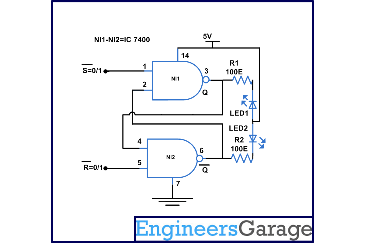
SR flip flop circuit using NAND gate is shown below. There are two input named S and R as shown in circuit diagram. To understand the working one must know the truth table of NAND gate. In NAND gate we will get output as 0 only if both the inputs are high and if any of the input is high or both the input is low we will receive logic 1. Working of SR flip is very simple.
Suppose we have applied S (NOT) =1 and R (NOT) =1 at the input of the flip flop the flip flop will not change its state and it will remain in its present state.
Suppose S (NOT) =0 and R (NOT)=1, the output of upper NAND gate become high. Thus both the inputs of lower NAND gate is high, output will be low. Therefore, we will receive 1 at reset input it will switch the flip flop to stable state where Q=1and Q(NOT) =0. In this state flip flop will set itself and at this time yellow LED will glow.
Now consider S (NOT) =1 and R (NOT)=0, now output of lower NAND gate become high making both the inputs of upper NAND gate high, Output will be low. Hence now we can say that a 1 at S (NOT) input sets the flip flop and flip flop switches to a stable state where Q=0 and Q(NOT) =1. In this state flip flop will set itself and at this time red LED will glow.
Now again consider both S (NOT) =0 and R (NOT)=0 at this time output of both the NAND gates to become high, both the output will be Q=1 and Q(NOT) =1 and this violates the definition of flip flop which says that both the outputs of a flip flop are complement of each other. Hence practically this condition is not possible in this both LED will not glow.
The above working of NAND gate as SR flip flop can be summarized in table as shown below-
|
S (NOT) |
R (NOT) |
Q |
State |
|
1 |
1 |
Previous State |
No change |
|
1 |
0 |
0 |
Reset |
|
0 |
1 |
1 |
Set |
|
0 |
0 |
? |
Forbidden |
Circuit Diagrams
Project Components
Project Video
Filed Under: Electronic Projects
Filed Under: Electronic Projects

Questions related to this article?
👉Ask and discuss on Electro-Tech-Online.com and EDAboard.com forums.
Tell Us What You Think!!
You must be logged in to post a comment.