Most chips that you see these days in servers, computers, and smartphones are composed of numerous smaller sized invisible chips. All these are closely sealed inside a single rectangular package that we call the chip.
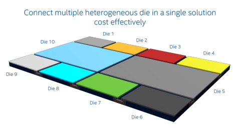
These microchips that form the larger chip for various electronic equipment including IO, memory, graphics card, CPU, server, etc. interact with each other through a very tiny innovation from Intel called the Embedded Multi-die Interconnect Bridge (EMIB).
Let’s understand EMIB
EMIB is a very complicated multi-layered sliver made up of silicon smaller than a single rice grain. It allows chips to transfer huge amount of data back and forth amidst all chips located next to each other at lightning speed which means a transfer of uncountable gigabytes per second.
Millions of high-quality laptops, field-programmable gate arrays, and several devices around the world work on this modus operandi. This number is estimated to soar to a billion as EMIB gets into the mainstream market. Remember, we talked about the Ponte Vecchio processor that was recently introduced as a general-purpose GPU, it is equipped with EMIB silicon.
How does it work?
EMIB enables chip makers and designers to bring together all specialized chips in a much faster manner. Previously, all chips used to sit over a single electronic baseboard with every single entity plugged into the package. The EMIB turns up the bandwidth by 85% while being cost-effective, small and flexible.
Its application in your graphics card, 5G processors, servers, and laptops will enhance the speed dramatically. And as the company will keep on engineering next versions of this device, it will further push the bandwidth to double and triple of present day figures.
Filed Under: News

Questions related to this article?
👉Ask and discuss on EDAboard.com and Electro-Tech-Online.com forums.
Tell Us What You Think!!
You must be logged in to post a comment.