A constant wave of innovations with organic Nanomaterials for usage in flexible electronics has viewers scratching their heads as to why they are not able to view more of such methodologies in applications like wearable electronics. The trouble has been that although organic Nanomaterials have introduced flexible logic displays and circuits possible, they have quite failed to introduce, non-volatile issues with erase/write speeds that would prepare them practical.
Now a group of scientists from the University of Strasbourg as well as from the Centre National de la Recherche Scientifique or CNRS in France, along with associated from University of Nova Gorica in Slovenia and Humboldt University of Berlin, has introduced a flexible optical non-volatile optical device sleek-film transistor gadget made from organic nanomaterials that may alter the arena in wearable electronics.
To date, the biggest challenge in introducing flexible organic memories has been preparing a stable system that does not reduce data over time (volatility), is flexible and provides an acceptable number of erase/write cycles.
The international research group concluded multiple hurdles, but they wanted more. “We desired every single gadget to be able to capture more than just a singular bit (multi-level process), we accomplished 8 bits,” says Emanuele Orgiu, a scientist at CNRS. “In addition, our gadgets can be prepared from solutions openly on a plastic substrate, and they characterize very instant response times (within nanonseconds) – a deeply sought-after property for organic semiconductors that usually showcase very lengthy response times (bigger than a millisecond),” says Orgiu.
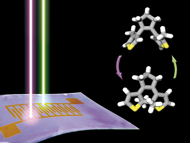
The group also explains that it was able to accomplish all of this by structuring the gadget from molecules called as diarylethenes or DAEs that can be shifted between two states, known as either closed or open form. Transferring from erasing to writing was as simple as regulating the wavelength off the light hitting the substance – green for erasing and blue for writing.
“The DAEs utilized in our work are specifically suitable for non-volatile information storage since their two types are stable at ambient conditions,” explains Tim Leydecker, another scientist from CNRS who is a member of the research group. “Also, they can be altered even when incorporated within a semiconducting polymer matrix, creating them an ideal candidature for flexible layers.”
The gadgets that they have structured so far are laboratory prototypes and hence are deliberately big at 1 square millimeter. No need to confirm the encapsulation and miniaturization will require being addressed so for such memories to become a marketable product. However, the scientists already have such troubles in their sights and think of continuing experimenting the stability and performance of the gadgets after encapsulation.
The group will also be identifying fabrication procedures matching with industrial output, like roll-to-roll creation and printing of ink-jet. Stefan Hecht, a group member from Humboldt University of Berlin, stated, “Implementation into electrical featuring other organic elements is a vital step, as the overall system would get benefitted from the advantages of organic electronics.”
Filed Under: News

Questions related to this article?
👉Ask and discuss on EDAboard.com and Electro-Tech-Online.com forums.
Tell Us What You Think!!
You must be logged in to post a comment.