
Representational image showing light-based computing.
The world of connectivity is currently passing through a major transformation as photons are being replaced by electrons in intercontinental fibre-optics based communications. Already the standard for intercontinental communication through fibre-optics, photons are replacing electrons as the main carriers of information throughout optical networks to computers.
Light is emerging as the primary vehicle for information processing in computers and telecommunications, particularly as the need for energy efficiency and bandwidth increases. But there are a few engineering barriers that challenge the completion of this transformation.
Industry-standard silicon circuits that support light are significantly larger than modern electronic transistors. One solution is to “compress” light by using metallic waveguides. However, this would require a new manufacturing infrastructure. Additionally, the way light interacts with metals on chips means that photonic information is easily lost.
Recently, scientists in Australia and Germany have developed a modular method to design nanoscale devices to overcome these problems, combining the best of traditional chip design with photonic architecture in a hybrid structure. Their research is published in Nature Communications.
“We have built a bridge between industry-standard silicon photonic systems and the metal-based waveguides that can be made 100 times smaller while retaining efficiency,” said lead author Dr Alessandro Tuniz from the University of Sydney Nano Institute and School of Physics.
This hybrid approach allows the manipulation of light at the nanoscale, measured in billionths of a meter. The scientists have shown that they can achieve data manipulation at 100 times smaller than the wavelength of light carrying the information.
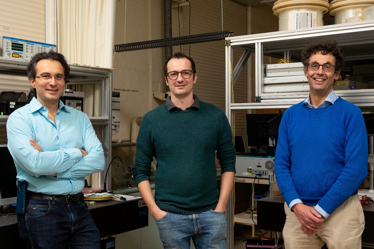
Research team: (from left) Associate Professor Stefano Palomba, Dr Alessandro Tuniz, Professor Martijn de Sterke. Photo: Louise Cooper
“This sort of efficiency and miniaturization will be essential in transforming computer processing to be based on light. It will also be very useful in the development of quantum-optical information systems, a promising platform for future quantum computers,” said Associate Professor Stefano Palomba, a co-author from the University of Sydney and Nanophotonics Leader at Sydney Nano.
On-chip nanometre-scale devices that use metals (known as “plasmonic” devices) allow for functionality unlike any other conventional photonic device. Notably, they efficiently compress light and achieve enhanced, interference-free, light-to-matter interactions.
“As well as revolutionising general processing, this is very useful for specialised scientific processes such as nano-spectroscopy, atomic-scale sensing and nanoscale detectors,” said Dr Tuniz also from the Sydney Institute of Photonics and Optical Science.
This modular approach allows for rapid rotation of light polarisation in the chip and, because of that rotation, quickly permits nano-focusing down to about 100 times less than the wavelength.
“We have shown that two separate designs can be joined together to enhance a run-of-the-mill chip that previously did nothing special,” Dr Tuniz said.
Filed Under: News

Questions related to this article?
👉Ask and discuss on Electro-Tech-Online.com and EDAboard.com forums.
Tell Us What You Think!!
You must be logged in to post a comment.