The dependency of the output with the inverting and non-inverting pin can be simply explained as below,
If the inverting pin is high compared to other pin, the output is negative
If the non-inverting pin is high compared to other pin, the output is positive
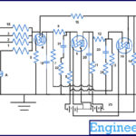
This pecularity of the input pins are demonstrated in the following circuit. Let us take a 741 op-amp IC and keep the inverting pin at a high potential compared to the non-inverting pin.


Fig. 3: Circuit Diagram of LM741 OPAMP IC based Non-Inverting Amplifier with High Inverting Pin
Contd…


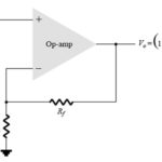
The non-inverting terminal
Non-inverting terminal Contd…

Proximity sensor


Capacitive touch switch
You can find touch switch in most of the high-end devices like mobile phones, laptops etc. The concept of the touch switch is very simple and in most of the cases capacitive touch is used.
In capacitive touch technology, when we touch the switch or a particular point in a touch screen, we are actually bringing our finger close to a sensing probe which is covered with some coating. When we actually touch, a capacitance will be generated between our finger and the touching probe which is separated by that coating. The device can sense that capacitance and hence a touch is detected.


Capacitive touch switch Contd…


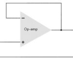
Concept of positive feedback


You may also like:
Filed Under: Featured Contributions

Questions related to this article?
👉Ask and discuss on Electro-Tech-Online.com and EDAboard.com forums.
Tell Us What You Think!!
You must be logged in to post a comment.