Astable multivibrator using op amp
Astable multivibrator is an electronic device which can continuously shift between its two states with respect to the output. If the output corresponding to one particular state is high, then the output corresponding to the other state is low. This nature of the circuit is useful in producing continuous output stream of pulses.
There is no need for external triggering in case of astable multivibrator circuits. Simply turn on the power and the circuit start oscillating between its two states. Since it is an oscillator, a positive feedback can be found in this kind of circuits also.
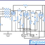
It is very easy to realize an astable multivibrator using op-amp ICs. The following circuit is an implementation of astable multivibrator using the 741 op-amp IC.

Fig. 1: Circuit Diagram of OPAMP based Multivibrator
In the above circuit, you can see a positive feedback introduced into the non-inverting pin of the 741 IC, after dividing the output voltage from pin6 using two resistors R1 and R2. There is a capacitor connected to the inverting pin of the op-amp. This capacitor charges through the pot RV1.
Initially the capacitor is uncharged condition, and we can expect 0V at the inverting pin of the op-amp. In this condition the output is high, and the non-inverting pin of the op-amp is getting a voltage, which is the output voltage divided by the two resistors. The capacitor starts charging to the high voltage of the output pin through the variable resistor RV1. While it is charging the potential at the inverting pin gradually increases. Eventually at some point of time, the voltage at the inverting pin reaches slightly above the voltage at the non-inverting pin. At this point of time the output of the op-amp goes low (negative) abruptly.
When the output pin becomes negative, the capacitor suddenly discharges to zero and then starts charging in the negative direction. While it charges in the negative direction, the output remains low since the non-inverting pin is getting a low voltage divided from the output pin. At some point of time the voltage at the inverting pin reaches below the voltage of the non-inverting pin and the output goes high (positive) abruptly.
Now the capacitor again discharges to zero and start doing the same procedure again. Thus we get a continuous pulse train at the output, and are indicated by the two LEDs.
Component specifications:
R1=R2=R3=1KE, 1/4W resistor
C1=10uf, 25V electrolytic capacitor
D1=LED (red), 3mm
D2=LED (green), 3mm
RV1=10K, variable resistor
U1=LM741
Component significance:
R1: The value of this resistor has significant effect in the time period of the output pulse. If you decrease this resistance, the output pulse’s time period increases and if you increase this resistance, the output pulse’s time period decreases.
R2: The pulse time period is directly depends on the value of this resistance. If you increase the resistance, the time period increases and if you decrease the resistance, the time period decreases.
R3: This resistance controls the brightness of the LEDs. Decreasing this resistance increases the brightness, and increasing this resistance decreases the brightness. The values above 220 ohms are safe to use with the LEDs.
C1: The output pulse time period keeps a direct proportionality with the value of this capacitance. If you increase the value, the time period increases and if you decrease the value the time period decreases.
RV1: The output pulse time period also has a direct proportionality with the value the resistance introduced by this variable resistance into the circuit. If you increase the resistance, the output time period increases and if you decrease the resistance, the output time period decreases.
Video
The inverting input terminal
The inverting input terminal
The inverting input terminal is what makes the op-amp differ from other normal amplifier circuits. An op-amp is designed for extremely high gain (ideally infinite), much more required than any practical applications. In order to make use in practical circuits for amplification of signals and voltages, this gain must be reduced to some comfortable levels. It can be done by providing a feedback of the output voltage to the inverting input pin.
Concept of negative feedback
In a negative feedback a fraction of the output voltage is subtracted from the applied input voltage so as to reduce the overall gain of the device. The negative feedback is normally used in amplifiers to reduce the gain and hence obtain the amplified output signal without any distortion due to waveform clipping occurs due to excess amplification. Negative feedback is also used to maintain the stability of the devices also.

Fig. 2: Block Diagram of Negative Feedback in OPAMP
As you can see from the symbolic representation of negative feedback from Figure: 35, the input voltage is added with a fraction of the inverted (negative) output voltage, which is produced by the device itself with gain A. The device with a negative gain B introduces the fraction of output voltage into the input terminal.
Incase of an op-amp the negative feedback is implemented by introducing a fraction of the output voltage to the inverting pin by means of a simple resistor.
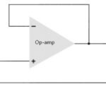
Here is an example showing the requirement of finite gain in amplifiers, and how the negative feedback can be implemented. Consider the following circuit in the Figure: 36

Fig. 3: Circuit Diagram of Operational Amplifier without Feedback
When you power on the above circuit, the LED will be glowing irrespective of the voltage you are applying at the non-inverting pin through the variable resistor. Even if you make the variable pin to the minimum, there is no effect on the LED. It will be glowing brighter and you will be wondering why? The reason is that, there is no feedback applied to the op-amp and it is now operating in its default higher gain. The gain is right now so high that even a minute voltage at the input pin can trigger a high output. Even if you vary the input voltage through a variable resistor there will be no effect on the output.
Component specifications:
R1=R2=R3=1K, 1/4 W
RV1=100K, Variable resistor
D1=LED (red), 3mm
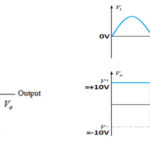
Now let’s assume that you are giving a sine wave as input to the non-inverting pin of the op-amp rather than varying the input using a variable resistor.

Fig. 4: Circuit Diagram of OPAMP based Sine Wave Generator without Feedback
In this case the output not only remains at maximum positive voltage, but goes to negative maximum also since the input sine wave has negative halves. The input waveforms and the resulting output waveforms for the above circuit are shown in the Figure: 38. These waveforms resemble that of the comparator circuit’s waveforms that we will be discussing later in this article.
Video
The inverting input terminal Contd…
As you can see that a sine wave input generates a square wave output, which means the input variations does not reflect in the output. This is the reason why this kind of circuit is not used for amplification of any natural waveforms. The output will be extremely distorted unless the amplifiers have finite gain.

Fig. 5: Signal Diagram of OPAMP based Sine Wave Generator without Feedback
The circuit shown in the Figure: 36 can be modified for finite gain by introducing a negative feedback. A resistance can be introduced between the output and the inverting input terminal of the amplifier and such a circuit is shown in the following figure.
In the circuit a variable resistance (RV2) of value 1K ohms is introduced to implement negative feedback in the circuit. This circuit has a finite gain and the gain can be adjusted by varying the resistance of RV2.
Now the output voltage is a product of input voltage with a finite gain. When you change the input voltage by varying the resistance, the brightness of the LED also varies accordingly. In this circuit the input variations are reflected in the output and even if you apply a sine wave in the input, you will get an amplified version of the same wave at the output. This kind of circuits can be used for amplifications of practical signal waveforms.

Fig. 6: Circuit Diagram of LM741 based Operational Amplifier with Negative Feedback
The image of an op-amp based amplifier circuit with negative feedback is shown in the following figure

Fig. 7: Image of of LM741 based Operational Amplifier with Negative Feedback
Inverting and non-inverting amplifiers
Inverting and non-inverting amplifiers
The op-amp amplifiers with negative feedback are basically classified into two types;
· Non-inverting amplifier and
· Inverting amplifier
Non-inverting amplifiers are negative feedback op-amp amplifiers in which the input signal is applied to the non-inverting input pin and the inverting pin is connected to the feedback system. Usually the feedback system will be a simple voltage divider using two resistors.
Fig. 8: Circuit Diagram of OPAMP based Non-Inverting Amplifier
In the above figure a non-inverting amplifier configuration is shown. The input voltage V1 is applied on the non-inverting pin of the op-amp. A feedback resistance Rf provides output voltage feedback to the inverting input. The resistors Rf and R1 combine to form a voltage divider for the output voltage. This voltage divider decides how much voltage should be added to the inverting input. Hence the gain of the amplifier reduces from ideally infinity to a particular constant value which depends on the resistance value of these two resistors.
If V1 is the input voltage at the non-inverting pin and V0 is the output voltage of the op-amp, then the gain of the non-inverting amplifier is given by the following equation.
Gain=V0/V1=(1+Rf/R1)
Inverting amplifiers are negative feedback op-amp amplifiers in which the input signal is applied to the inverting input pin itself along with the feedback system on the same pin. Usually the feedback system will be a simple voltage divider using two resistors.

Fig. 9: Circuit Diagram of Inverting Amplifier
In the above figure an inverting amplifier configuration is shown. The input voltage V1 is applied on the inverting pin of the op-amp. A feedback resistance Rf provides output voltage feedback to the inverting input. The resistors Rf and R1 combine to form a voltage divider for the output voltage. This voltage divider decides how much voltage should be added to the inverting input along with the input voltage. Hence the gain of the amplifier reduces from ideally infinity to a particular constant value which depends on the resistance value of these two resistors. The non-inverting pin is normally grounded.
If V1 is the input voltage at the inverting pin and V0 is the output voltage of the op-amp, then the gain of the non-inverting amplifier is given by the following equation.
Gain=V0/V1= -(Rf/R1)
You might have noticed that there is a negative symbol in the above gain equation. The reason is nothing but the output will be negative since the non-inverting pin is grounded and we are applying a voltage on the inverting pin. In case of input signals other than DC voltages, the output wave will be having a 180 degree phase shift with respect to the waves.
You may also like:
Filed Under: Featured Contributions

Questions related to this article?
👉Ask and discuss on Electro-Tech-Online.com and EDAboard.com forums.
Tell Us What You Think!!
You must be logged in to post a comment.