This chapter deals with the objective and unique features of the project and the organisation of the report.
1.2 OBJECTIVE
The objective of the project work is to build an aid for physically challenged people to enable them operate normal daily life gadgets easily and conveniently using a voice recognition system and embedded controllers. The application chosen is on GSM MODEM, on which basic mobile phone operations are performed.
1.3 EXISTING TECHNOLOGY
In today’s generation mobile phone has become essential equipment for communication. In mobiles we have a special feature called voice tag which helps a user to store voice note for a corresponding contact. Whenever the user repeats that voice note the corresponding number of that contact will be dialed. This makes the user to call the numbers using their voices easily.
1.4 DRAWBACKS OF THE EXISTING SYSTEM
In currently existing technology we cannot call or store a new number in the database using voice input. The reason is that when you give some voice inputs it simply samples and stores it in the form of digital data. It doesn’t have the capacity to identify the characters present in that voice input. This has been the major drawback because all programming language requires a string of characters, which helps in doing necessary operation like storing a name or number.
1.5 HOW TO OVERCOME THIS DRAWBACK
We have solved this problem by simply allocating separate voice tags for all alphabets, numbers and some special commands. So, whenever a person wants to perform any operation he will simply say the required command followed by spelling the required characters one after the other.
During the time duration between each character that are being spelled out, the character tag will be identified and the corresponding characters will be generated in the microcontroller. After recognizing the required command (a set of characters) to accept voice input, the characters that are recognized will be converted into string. This string of characters will then be used to do the required operation like storing, calling, retrieving etc.
1.6 UNIQUE FEATURES OF THE PROJECT
· Single chip voice recognition circuit capable of recognizing characters to generate the string of characters with the help of microcontroller.
· Can be operated in any language as the user’s wish.
· Highly secured as the user alone knows what is the language used to operate the kit.
· Unique phonebook feature operated by voice.
· Information about the caller.
· Basic mobile phone operations like storing, retrieving, deleting and calling can be performed.
CHAPTER – 2
Block Diagram Description
2.1 GENERAL:
This chapter deals with the overall block diagram and the overview of each module which should be interfaced to make a call to a required number and also to retrieve the phone number of the person who is calling the user.
 Fig 2.2 Overall Block Diagram
Overall Circuit Diagram: Check Circuit Diagram 1 Tab.
2.4 OVERVIEW OF MODULES
The task is divided into following modules.
1. Voice Recognition Circuit.
2. Dialing circuit
2.4.1 Voice Recognition Circuit:
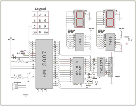
This kit is used for storing and recognizing the voice. This kit contains HM2007 IC, DTMF keypad, RAM, latches, 7 segment decoder and 7 segment display. Using these components the voice is stored and recognized.
2.4.2 Dialing Circuit:
It consists of a decoded GSM modem. Here each and every button are decoded and their inputs are given to relays which helps in making that corresponding button to be enabled by energizing the coil of the corresponding enabled by triggering the corresponding relay and a call is made to that number.
2.5 POWER SUPPLY
2.5.1. Power Supply – An Introduction
The power supply is very important section of all electronic devices as all the electronic devices works only in DC. One important aspect of the project is that the power supply should be compact. Most electronic devices need a source of DC power.
Power supply unit consists of following units:
1. Step down transformer
2. Rectifer unit
3. Input filter
4. Regulator unit
5. Output filter
The circuit is powered by a 12V dc adapter, which is given to LM7805 voltage regulator by means of a forward voltage protection diode and is decoupled by means of a 0.1 uf capacitor. The voltage regulator gives an output of exactly 5V dc supply. The 5V dc supply is given to all the components including the Microcontroller, the serial port, and the IR transmitters and sensors.
The AC supply which when fed to the step down transformer is leveled down to 12 volts AC. This is then fed to full wave rectifer which converts it in to 12 volts DC. This is then passed to a filter to remove the ripples. Then it is fed to a voltage regulator that converts 12 V to 5 V stable voltages and currents.
2.5.2. Step-down Transformer
The step down transformer is used to step down the main supply voltage from 230AC to lower value. This 230AC voltage cannot be used directly, thus its stepped down. The transformer consists of primary and secondary coils. To reduce or step down the voltage, the transformer is designed to contain less number of turns in its secondary core. Thus the conversion from AC to DC is essential. This conversion is achieved by using the rectifier circuit.
2.5.3. Rectifier Unit
The Rectifier circuit is used to convert AC voltage into its corresponding DC voltage. There are Half-Wave and Full-Wave rectifiers available for this specific function. The most important and simple device used in rectifier circuit is the diode. The simple function of the diode is to conduct when forward biased and not to conduct when reverse biased. The forward bias is achieved by connecting the diode’s positive with of positive of battery and negative with battery’s negative. The efficient circuit used is full wave bridge rectifier circuit. The output voltage of the rectifier is in rippled form, the ripples from the obtained DC voltage are removed using other circuits available. The circuit used for removing the ripples is called Filter circuit.
2.5.4. Input Filter
Capacitors are used as filters. The ripples from the DC voltage are removed and pure DC voltage is obtained. The primary action performed by capacitor is charging and discharging. It charges in positive half cycle of the AC voltage and it will discharge in its negative half cycle, so it allows only ACC voltage and does not allow the DC voltage. This filter is fixed before the regulator. Thus the output is free from ripples.
2.5.5. Regulator Unit
Regulator regulates the output voltage to be always constant. The output voltage is maintained irrespective of the fluctuations in the input AC voltage. As and then the AC voltage changes, the DC voltage also changes. To avoid this, regulators are used. Also when the internal resistance of the power supply is greater than 30 ohms, the pull up gets affected. Thus this can be successfully reduced here. The regulators are mainly classified for low voltage and for high voltage.
2.5.6. IC Voltage Regulators
Voltage regulators comprise a class of widely used ICs. Regulator IC units contain the circuitry for reference source, comparator amplifier, control device and overload protection all in a single IC. Although the internal construction of the IC somewhat is different from that described for discrete voltage regulator circuits, the extenal operation is much the same. IC units provide the regulation of a fixed positive voltage, a fixed negative voltage or an adjustably set voltage.
A Power Supply can be built using a transformer connected to the AC supply line to step the ac voltage to desired amplitude, then rectifying that ac voltage using IC regulator. The regulators can be selected for operation with load currents from hundreds of milli amperes to tens of amperes, corresponding to power ratings from milli watts to tens of watts.
The purpose of the regulator is to maintain the output voltage constant irrespective of the fluctuations in the input voltage. The Micro controller and PC work at a constant supply voltage of +5V,-5Vand +12V and -12V respectively. The regulators are mainly classified for positive and negative voltage.
2.5.7. LM 7805 Voltage Regulator
Features
1. Output Current up to 1A
2. Output Voltages of 5, 6, 8, 9, 10, 11, 12, 15, 18, 24V
3. Thermal Overload Protection
4. Short Circuit Protection
5. Output Transistor Safe Operating area Protection
Description
The MC78XX/LM78XX series of three-terminal positive regulators are available in the TO-220/D-PAK package and with several fixed output voltages, making them useful in a wide range of application.
Each type employs internal current limiting, thermal shut-down and safe operating area protection, making it essentially indestructible. If adequate heat sinking is provided, they can deliver over 1A output current.
2.5.8 Output Filter
The filter circuit is often fixed after the regulator circuit. Capacitor is most often used as filter. The principle of the capacitor is to charge and discharge. It charges during the positive half cycle of the AC voltage and discharges during the negative half cycle. So it allows AC voltage and not DC voltage. This filter is fixed after the regulator circuit to filter any of the possibly found ripples in the output received finally. The output at this stage is 5V and is given to Microcontroller 89S52.
CHAPTER 3
Atmel Microcontroller
Chapter three deals about the microcontrollers. Refer the below links for the details of the microcontroller:
http://www.engineersgarage.com/microcontroller
http://www.engineersgarage.com/8051-microcontroller
http://www.engineersgarage.com/electronic-components/at89c51-microcontroller-datasheet
http://www.engineersgarage.com/sites/default/files/AT89C51.pdf
Chapters 4
Descriptions of Voice Recognition Kit & Dialing Circuit
4.1 GENERAL:
This chapter deals with the brief descriptions of various modules that are necessary to call a required number with the help of voice input. The modules are voice recognition circuit and dialer circuit.
4.2 VOICE RECOGNITION CIRCUIT:
4.2.1 GENERAL:
This kit is used for storing and recognizing the voice.HM2007 is a 48 pin single chip cmos voice recognition LSI circuit with on chip analog front end, voice analysis, recognition process and system control function
During the training period the input voices are stored into a specified location in the RAM with the help of HM2007 & keypad. Similarly, when the characters are spelled out the corresponding location of character is displayed in the seven-segment display and it is also sent to the ATMEL controller.
4.2.2 WORKING OF VOICE RECOGNITION CIRCUIT:
Figure in Circuit Diagram 2 tab describes the circuit diagram of the voice recognition kit. HM2007 IC has the capacity to recognize 40 isolated characters. There are two modes namely Training and recognition. During the training period (mode), the input voices are stored in the specified locations of the RAM with the help of HM2007 & keypad. During the recognition mode when the voice input is given through mic, the corresponding location of that voice input in the RAM is displayed in the seven-segment display and it is also sent to the PIC controller for further processing.
4.2.3 COMPONENTS REQUIRED
• KEYPAD
• HM2007 IC
• HY6264A RAM
• SN74LS373N LATCH
• SN74LS47N 7 SEGMENT DECODER – 2NOs
• 7 SEGMENT DISPLAY – 2NOs
4.2.3.1 KEYPAD
The keypad consists of 0-9 keys, clear key in the bottom left corner and training key in the bottom right corner.
4.2.3.2 HM2007 IC
It has two basic modes of operation training and recognition mode. During the training mode the input voice is stored into a specified location in the RAM with the help of HM2007 & keypad. When the characters are spelled out the corresponding location of character is displayed in the seven-segment display and it is also sent to the ATMEL controller.
4.2.3.3 HY6264A RAM
It is a 8K RAM used to store the data from HM2007IC.The memory locations will be allocated automatically by the HM2007IC.
4.2.3.4. SN74LS373N LATCH:
It is used to get the output to microcontroller and 7-segment decoder. When DE signal is enabled output is obtained at the latch.
4.2.3.5 7 SEGMENT DECODER:
A decoder is a device which does the reverse of an encoder, undoing the encoding so that the original information can be retrieved. The same method used to encode is usually just reversed in order to decode.
A decoder can take the form of a multiple-input, multiple-output logic circuit that converts coded inputs into coded outputs, where the input and output codes are different. e.g. n-to-2n, binary-coded decimal decoders. Enable inputs must be on for the decoder to function, otherwise its outputs assume a single “disabled” output code word. Decoding is necessary in applications such as data multiplexing, 7 segment display and memory address decoding.
It is used to decode the hexadecimal inputs to corresponding 7-segment display from the latch.
4.2.3.6 7 SEGMENT DISPLAY:
A seven segment display, as its name indicates, is composed of seven elements.
In most applications, the seven segments are of nearly uniform shape and size (usually elongated hexagons, though trapezoids and rectangles can also be used), though in the case of adding machines, the vertical segments are longer and more oddly shaped at the ends in an effort to further enhance readability.
Each of the numbers 0, 6, 7 and 9 may be represented by two or more different glyphs on seven-segment displays.
IN the project the seven segments are arranged as a rectangle of two vertical segments on each side with one horizontal segment on the top, middle, and bottom. Additionally, the seventh segment bisects the rectangle horizontally. There are also fourteen-segment displays and sixteen-segment displays (for full alpha numeric); however, these have mostly been replaced by dot-matrix displays.
Seven-segment displays may use a liquid crystal display (LCD), arrays of light emitting diodes (LEDs), or other light-generating or controlling techniques such as cold cathode gas discharge, vacuum fluorescent, incandescent filaments, and others.
There are two 7 segment display available used to display the two digit numbers entered through the keypad and from HM2007IC.
Numbers to 7-segment-code
A single byte can encode the full state of a 7-segment-display. The most popular bit encodings are gfedcba and abcdefg – both usually assume 0 is off and 1 is on.
This table gives the hexadecimal encodings for displaying the digits 0 to F:
|
Digit |
gfedcba |
abcdefg |
a |
b |
C |
d |
e |
f |
g |
|
0 |
0x3F |
0x7E |
on |
on |
on |
on |
on |
on |
off |
|
1 |
0x06 |
0x30 |
off |
on |
on |
off |
off |
off |
off |
|
2 |
0x5B |
0x6D |
on |
on |
off |
on |
on |
off |
on |
|
3 |
0x4F |
0x79 |
on |
on |
on |
on |
off |
off |
on |
|
4 |
0x66 |
0x33 |
off |
on |
on |
off |
off |
on |
on |
|
5 |
0x6D |
0x5B |
on |
off |
on |
on |
off |
on |
on |
|
6 |
0x7D |
0x5F |
on |
off |
on |
on |
on |
on |
on |
|
7 |
0x07 |
0x70 |
on |
on |
on |
off |
off |
off |
off |
|
8 |
0x7F |
0x7F |
on |
on |
on |
on |
on |
on |
on |
|
9 |
0x6F |
0x7B |
on |
on |
on |
on |
off |
on |
on |
|
A |
0x77 |
0x77 |
on |
on |
on |
off |
on |
on |
on |
|
B |
0x7C |
0x1F |
off |
off |
on |
on |
on |
on |
on |
|
C |
0x39 |
0x4E |
on |
off |
off |
on |
on |
on |
off |
|
D |
0x5E |
0x3D |
off |
on |
on |
on |
on |
off |
on |
|
E |
0x79 |
0x4F |
on |
off |
off |
on |
on |
on |
on |
|
F |
0x71 |
0x47 |
on |
off |
off |
off |
on |
on |
on |
CHAPTER 5
WORKING OF GSM MODEM
5.1 GENERAL
GSM (Global System for Mobile communications: originally from Groupe Special Mobile) is the most popular standard for mobile phones in the world. Its promoter, the GSM Association, estimates that 80% of the global mobile market uses the standard. GSM is used by over 3 billion people across more than 212 countries and territories.
Its ubiquity makes international roaming very common between mobile phone operators, enabling subscribers to use their phones in many parts of the world. GSM differs from its predecessors in that both signaling and speech channels are digital, and thus is considered a second generation (2G) mobile phone system.
This has also meant that data communication was easy to build into the system. GSM EDGE is a 3G version of the protocol.
The ubiquity of the GSM standard has been an advantage to both consumers (who benefit from the ability to roam and switch carriers without switching phones) and also to network operators (who can choose equipment from any of the many vendors implementing GSM).
GSM also pioneered a low-cost (to the network carrier) alternative to voice calls, the short message service (SMS, also called “text messaging”), which is now supported on other mobile standards as well. Another advantage is that the standard includes one worldwide emergency telephone number, 112.
This makes it easier for international travellers to connect to emergency services without knowing the local emergency number. 22
5.2 SIM300 GSM
Designed for global market, SIM300 is a Tri-band GSM/GPRS engine that works on frequencies EGSM 900 MHz, DCS 1800 MHz and PCS1900 MHz SIM300 provides GPRS multi-slot class 10 capabilities and support the GPRS coding schemes CS-1, CS-2, CS-3 and CS-4.
With a tiny configuration of 40mm x 33mm x 2.85 mm, SIM300 can fit almost all the space requirement in your application, such as Smart phone, PDA phone and other mobile device. The SIM300 is designed with power saving technique, the current consumption to as low as 2.5mA in SLEEP mode. 23
5.3. MAX 232
The MAX 232 IC is used to communicate between the Microcontroller and the PC. The capacitors around the max232 IC is used primarily for charge pumping the voltage from the Microcontroller to the PC. The MAX232 line driver/receiver is intended for all EIA/TIA-232E and V.28/V.24 communications interfaces, and in particular, for those applications where ±12V is not available. It contains 2 RS-232 drivers and 2 receivers. The MAX232 operates from a single +5V power supply. This part is especially useful in battery-powered systems since its low-power shutdown mode reduces power dissipation to less than 5mW.
The Microcontroller can work at only logic levels of minimum 0v & maximum of 5v and PC works at voltage levels of minimum -12v to +12v. For the serial port communication to take place between the microcontroller and the PC the voltage levels have to be converted. MAX232 converter is responsible to do this conversion. The PC works with RS232 standard while the microcontroller works in the TTL logic. The level converter IC MAX232 is used for the conversion from the TTL logic to the RS232 logic.
The MAX232 line driver/receiver is intended for all EIA/TIA-232E and V.28/V.24 communications interfaces, and in particular, for those applications where ±12V is not available. It contains 2 RS-232 drivers and 2 receivers.
The MAX232 operates from a single +5V power supply. This part is especially useful in battery-powered systems since its low-power shutdown mode reduces power dissipation to less than 5mW.
5.4. WORKING
The Microcontroller can work at only logic levels of minimum 0v & maximum of 5v and PC works at voltage levels of minimum -12v to +12v. For the serial port communication to take place between the microcontroller and the PC the voltage levels have to be converted. MAX232 converter is responsible to do this conversion.
The MAX232 line driver/receiver is intended for all EIA/TIA-232E and V.28/V.24 communications interfaces, particularly applications where ±12V is not available. These parts are especially useful in battery-powered systems, since their low-power shutdown mode reduces power dissipation to less than 5µW. The MAX232 use no external components and are recommended for applications where printed circuit board space is critical.
5.5. Applications
• Portable Computers
• Low-Power Modems
• Interface Translation
• Battery-Powered RS-232 Systems
• Multi drop RS-232 Networks
The MAX232 contain four sections: dual charge-pump DC-DC voltage converters, RS-232 drivers, RS-232 receivers, and receiver and transmitter enable control inputs.
5.6. Dual Charge-Pump Voltage Converter
The MAX232 have two internal charge-pumps that convert +5V to ±10V (unloaded) for RS-232 driver operation. The first converter uses capacitor C1 to double the +5V input to +10V on C3 at the V+ output. The second converter uses capacitor C2 to invert +10V to-10V on C4 at the V- output. A small amount of power may be drawn from the +10V(V+) and -10V (V-) outputs to power external circuitry.
V+ and V- are not regulated, so the output voltage drops with increasing load current. Do not load V+ and V- to a point that violates the minimum ±5V EIA/TIA-232E driver output voltage when sourcing current from V+ and V- to external circuitry.
5.7. RS-232 Drivers
The typical driver output voltage swing is ±8V when loaded with 5k. RS-232 receiver and VCC =+5V. Output swing is guaranteed to meet the EIA/TIA-232E and V.28 specification, which calls for ±5V minimum driver output levels under worst-case conditions. Input thresholds are both TTL and CMOS compatible.
The inputs of unused drivers can be left unconnected since 400k. input pull-up resistors to VCC are built-in (except for the MAX220).The pull-up resistors force the outputs of unused drivers low because all drivers invert. The internal input pull-up resistors typically source 12µA, except in shutdown mode where the pull-ups are disabled. Driver outputs turn off and enter a high-impedance state—where leakage current is typically microamperes (maximum 25µA)—when shut down is removed. Outputs can be driven to ±15V. The power supply current typically drops to 8µA in shutdown mode. The MAX220 does not have pull-up resistors to force the outputs of the unused drivers low. Connect unused inputs to GND or VCC.
Chapter 6
SOFTWARE DESCRIPTION
6.1 TYPES OF TOOLS:
KEIL C
ORCAD
· Capture
· Layout
6.1.1 KEIL C:
Keil software is the leading vendor for 8/16-bit development tools (ranked at first position in the 2004 embedded market study of the embedded system and EE times magazine).
Keil software is represented world wide in more than 40 countries, since the market introduction in 1988; the keil C51 compiler is the de facto industry standard and supports more than 500 current 8051 device variants. Now, keil software offers development tools for ARM.
Keil software makes C compilers, macro assemblers, real-time kernels, debuggers, simulators, integrated environments, and evaluation boards for 8051, 251, ARM and XC16x/C16x/ST10 microcontroller families.
The Keil C51 C Compiler for the 8051 microcontroller is the most popular 8051 C compiler in the world. It provides more features than any other 8051 C compiler available today.
The C51 Compiler allows you to write 8051 microcontroller applications in C that, once compiled, have the efficiency and speed of assembly language. Language extensions in the C51 Compiler give you full access to all resources of the 8051.
The C51 Compiler translates C source files into relocatable object modules which contain full symbolic information for debugging with the µVision Debugger or an in-circuit emulator. In addition to the object file, the compiler generates a listing file which may optionally include symbol table and cross reference
· Nine basic data types, including 32-bit IEEE floating-point,
· Flexible variable allocation with bit, data, bdata, idata, xdata, and pdata memory types,
· Interrupt functions may be written in C,
· Full use of the 8051 register banks,
· Complete symbol and type information for source-level debugging,
· Use of AJMP and ACALL instructions,
· Bit-addressable data objects,
· Built-in interface for the RTX51 real time kernels,
· Support for the Philips 8xC750, 8xC751, and 8xC752 limited instruction sets,
· Support for the Infineon 80C517 arithmetic unit.
6.2 GENERAL
This chapter deals with algorithms.
6.3 CHARACTERS RECOGNITION AND EXTRACTION IN MICROCONTROLLER
Step1: Switch on the device.
Step2: Train the characters in the specified location during the training period of the voice recognition kit.
Step3: During the recognition period when the characters are spelled their corresponding location number will be given to ATMEL microcontroller as input.
Step4: When the input matches with the predefined BCD numbers their corresponding alphabets will be generated and stored in a stack.
Step5: All the characters that are spelled are recognized in such a way and their corresponding characters are taken out and they are stored in the stack and finally deployed as a string and stored in the memory.
Step6: These stored strings are then used for various operations like calling, playing the character, matching the numbers etc.
Step7: Switch off once the corresponding operations are done.
6.4 DIALING A NUMBER
6.4.1 DIALING A STORED NUMBER
Step 1: Start the program.
Step 2: Check the input.
Step 3: If the input is equal to call then get the name of the person.
Step 4: If the name is present in the database then call the corresponding number using dialing circuit by enabling the corresponding relays for each number.
Step 5: If the input is not equal to call then go to step 2.
Step 6: End the program.
6.4.2 DIALING A NEW NUMBER
Step 1: Start the program.
Step 2: Check the voice input.
Step 3: If the input is equal to new then get the number to be dialed.
Step 4: Then call the corresponding number using dialing circuit by enabling the corresponding relays for each number.
Step 5: End the program.
Chapter 8
CONCLUSION AND FUTURE WORK
8.1 CONCLUSION
A mobile aid for physically challenged people to operate their normal landline telephone has been developed. The kit uses a voice recognition system and embedded controllers to perform the required operations satisfactorily.
8.2 FUTURE WORK
In mobile phones we have a facility called voice tag, in which we can only record our voice to the contacts that are available in the memory. We cannot store a number using our voice that is not present in the contact. Similarly we cannot delete a number using the voice.
In future, it can all be implemented using a user’s voice with the help of voice recognition embedded controller, which can be incorporated in mobile phone. Thus, mobile phones can be made to operate completely without the help of a person’s hand. By this the physically challenged people other than the people who cannot speak and hear can use mobile phone without the help of other people.
You may also like:


Project Source Code
###
#include
void main()
{
unsigned char i;
SCON=0x50;
TMOD=0x20;
TH1=0xfd;
TR1=1;
P1=0xff;
P3=0x0F;
del1();
delay1();
while(1)
{
if(P1==0x01)
{
txs('A');txs('T');txs(13); txs(10);
delay1();
}
if(P1==0x02)
{
txs('A');txs('T');txs('H');txs(13); txs(10); //Hang Up
delay1();
}
if(P1==0x03)
{
txs('A');txs('T');txs('A');txs(13); txs(10); //Attend
delay1();
}
if(P1==0x04)
{
}
if(P1==0x05)
{
}
if(P1==0x06)
{
txs('A');txs('T');txs('D');
txs('8');txs('8');txs('2');txs('5');
txs('5');txs('7');txs('1');txs('5');txs('5');txs('9');txs(';');
txs(13); txs(10);
delay1();
}
if(P1==0x07)
{
txs('A');txs('T'); txs('D');
txs('9');txs('4');txs('4');txs('4');
txs('3');txs('4');txs('2');txs('3');txs('2');txs('5');txs(';');
txs(13); txs(10);
delay1();
}
if(P1==0x08)
{
txs('A');txs('T'); txs('D');
txs('9');txs('0');txs('0');txs('3');
txs('1');txs('2');txs('9');txs('8');txs('7');txs('6');txs(';');
txs(13); txs(10);
delay1();
}
if(P1==0x09)
{
txs('A');txs('T'); txs('D');
}
if(P1==0x10)
{
txs('0');
}
if(P1==0x11)
{
txs('1');
}
if(P1==0x12)
{
txs('2');
}
if(P1==0x13)
{
txs('3');
}
if(P1==0x14)
{
txs('4');
}
if(P1==0x15)
{
txs('5');
}
if(P1==0x16)
{
txs('6');
}
if(P1==0x17)
{
txs('7');
}
if(P1==0x18)
{
txs('8');
}
if(P1==0x19)
{
txs('9');
}
if(P1==0x20)
{
txs(';');txs(13); txs(10);
delay1();
}
###
Circuit Diagrams

Filed Under: Electronic Projects

Questions related to this article?
👉Ask and discuss on EDAboard.com and Electro-Tech-Online.com forums.
Tell Us What You Think!!
You must be logged in to post a comment.