Engineers Garage

  • Electronic Projects & Tutorials
    • Electronic Projects
      • Arduino Projects
      • AVR
      • Raspberry pi
      • ESP8266
      • BeagleBone
      • 8051 Microcontroller
      • ARM
      • PIC Microcontroller
      • STM32
    • Tutorials
      • Audio Electronics
      • Battery Management
      • Brainwave
      • Electric Vehicles
      • EMI/EMC/RFI
      • Hardware Filters
      • IoT tutorials
      • Power Tutorials
      • Python
      • Sensors
      • USB
      • VHDL
    • Circuit Design
    • Project Videos
    • Components
  • Articles
    • Tech Articles
    • Insight
    • Invention Stories
    • How to
    • What Is
  • News
    • Electronic Product News
    • Business News
    • Company/Start-up News
    • DIY Reviews
    • Guest Post
  • Forums
    • EDABoard.com
    • Electro-Tech-Online
    • EG Forum Archive
  • DigiKey Store
    • Cables, Wires
    • Connectors, Interconnect
    • Discrete
    • Electromechanical
    • Embedded Computers
    • Enclosures, Hardware, Office
    • Integrated Circuits (ICs)
    • Isolators
    • LED/Optoelectronics
    • Passive
    • Power, Circuit Protection
    • Programmers
    • RF, Wireless
    • Semiconductors
    • Sensors, Transducers
    • Test Products
    • Tools
  • Learn
    • eBooks/Tech Tips
    • Design Guides
    • Learning Center
    • Tech Toolboxes
    • Webinars & Digital Events
  • Resources
    • Digital Issues
    • EE Training Days
    • LEAP Awards
    • Podcasts
    • Webinars / Digital Events
    • White Papers
    • Engineering Diversity & Inclusion
    • DesignFast
  • Guest Post Guidelines
  • Advertise
  • Subscribe

PCB Designing using Diptrace Software: Step by Step Tutorial

By Abbas April 21, 2008


The efficient laying out of traces on a PCB is a complex skill, and requires much patience. This task has been made vastly easier with the advent of readily available PCB layout software, but it is still challenging.

Usually an electronics or electrical engineer designs the circuit, and a layout specialist designs the PCB. PCB design is a specialized skill. There are numerous techniques and standards used to design a PCB that is easy to manufacture and yet small and inexpensive.

There are various types of software which are used for PCB designing, In PCB designing first think what is required, a Schematic diagram of the circuit then we have to make a layout by using software and this layout gets printed on the PCB after that Etching, drilling, component placement and soldering are done.

In this tutorial we use Diptrace (version 2.0.1.7) Software for Layout designing, it is a free software and you can download it from Diptrace official website.
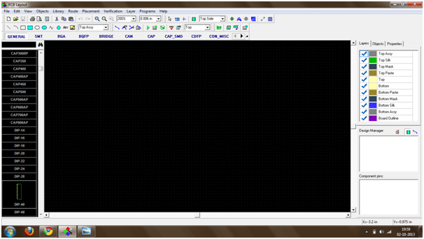
Screenshot of Diptrace Software used for Layout Design

Fig. 1: Screenshot of Diptrace Software used for Layout Design

Schematic Circuit:

First we required a circuit diagram which we are going to make on a PCB. So in this tutorial we are going to make 555 timer astable mode circuit. Circuit diagram is shown in the below image
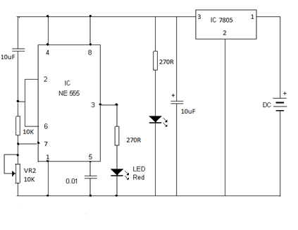
Image of a sample circuit diagram

Fig. 2: Image of a sample circuit diagram

Installing the Software

Software Description:

Installation of Software

Screenshot of installing Diptrace on Windows

Fig. 3: Screenshot of installing Diptrace on Windows

After installation, open PCB layout in Diptrace Software.

Screenshot of launching Diptrace from Windows Start Menu

Fig. 4: Screenshot of launching Diptrace from Windows Start Menu

On opening software, the window looks like this. In that there are components blocks, In general window we find all the components which are generally used for layout. Other windows like SMT, Bridge, can, Capacitor and all other blocks.

Screenshot of Diptrace Software used for Layout Design

Fig. 5: Screenshot of Diptrace Software used for Layout Design

How to insert component

To pick a component left click on the components and drag it onto the screen and drop. To leave a components right click on the screen then next components are get placed.

Screenshot of inserting a component on Diptrace

Fig. 6: Screenshot of inserting a component on Diptrace

To change a name of the components right click on the components and change the name as we want to write.

Screenshot of naming a component on Diptrace

Fig. 7: Screenshot of naming a component on Diptrace

Screenshot of naming a component on Diptrace

Fig. 8: Screenshot of naming a component on Diptrace

Screenshot of renamed component on Diptrace

Fig. 9: Screenshot of renamed component on Diptrace

Screenshot of more components added to layout on Diptrace

Fig. 10: Screenshot of more components added to layout on Diptrace

There are two side of the PCB that is Top and Bottom, in top we see the components name and details and in bottom we see only pad.
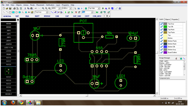
Screenshot of top view of layout on Diptrace

Fig. 11: Screenshot of top view of layout on Diptrace

We can also rotate the components if we want to arrange components in a systematic manner.

Screenshot of rotating a component on Diptrace

Fig. 12: Screenshot of rotating a component on Diptrace

Manual Routing

There are two type of Routing in Diptrace software that is Manual Routing and automatic routing. First we see manual routing, for manual routing, select bottom view and click on route manual button then draw the layout as we want to connect.

Screenshot of manual routing on Diptrace

Fig. 13: Screenshot of manual routing on Diptrace

Then arrange all the components and start drawing layouts, by this we can be able to draw a complete layout of our circuit.

Bottom View of the layout
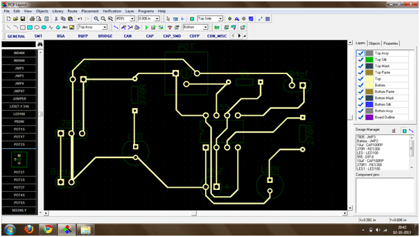
Screenshot of bottom view of layout on Diptrace

Fig. 14: Screenshot of bottom view of layout on Diptrace

Top view of the Layout.

Screenshot of top view of layout on Diptrace

FIg. 15: Screenshot of top view of layout on Diptrace

Next we will see how to draw a layout by using automatic routing tool.

Automatic Routing

For automatic routing we didn’t required to select any tool, just draw the connection from the top menu itself.
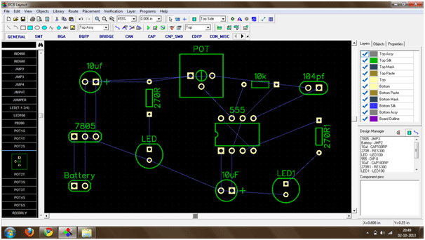
Screenshot of Automatic Routing on Diptrace

Fig. 16: Screenshot of Automatic Routing on Diptrace

The connections are done as we see in image. Before doing auto routing we have to do some setting on the software, click on route menu button then click on auto router setup button as we see in image shown below.

Screenshot of Route Menu on Diptrace

Fig. 17: Screenshot of Route Menu on Diptrace

Then click on use priority layer direction button.

Screenshot showing priority layer direction button in Route options

Fig. 18: Screenshot showing priority layer direction button in Route options

After that do setting, for set the direction of top menu in off mode as we shown in image.

Screenshot of setting top view off in Diptrace settings

Fig. 19: Screenshot of setting top view off in Diptrace settings

After doing this setting click on the run auto router menu or press F9.
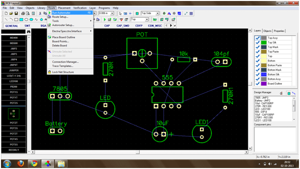
Screenshot of running auto router on Diptrace

Fig. 20: Screenshot of running auto router on Diptrace

After pressing on run auto router button a small routing process performed after that we get layout of our schematic circuit.

Screenshot of an auto routed layout on Diptrace

Fig. 21: Screenshot of an auto routed layout on Diptrace

The bottom (Layout) of the schematic circuit is shown in image.
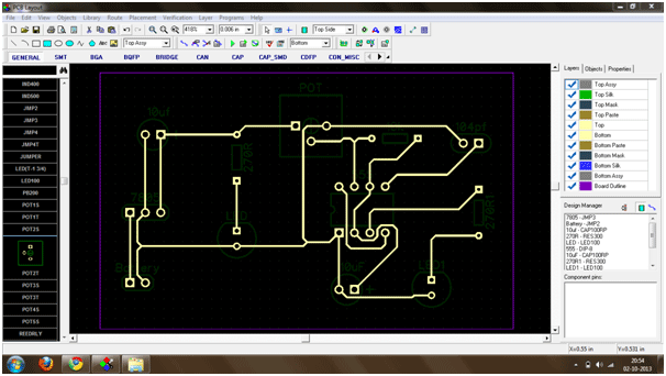
Screenshot of the bottom view of layout on Diptrace

Fig. 22: Screenshot of the bottom view of layout on Diptrace

layout is ready to print on PCB but we can also place copper pour on the PCB, copper pour is very useful for complex circuit to reduce the complexity as well as for simplicity of our layout. First let’s see how to select place copper pour menu.
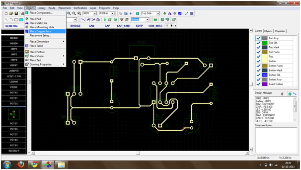
Screenshot of placing copper pour from Route menu on Diptrace

Fig. 23: Screenshot of placing copper pour from Route menu on Diptrace

After selecting the tool we have to cover the layout on the rectangular box, and then right click on the corner as we shown in image.
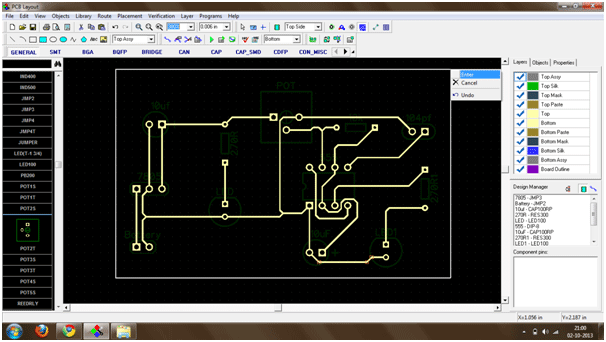
Screenshot of drawing layout boundaries on Diptrace

Fig. 24: Screenshot of drawing layout boundaries on Diptrace

Then increase the clearance.

Screenshot of copper pour settings on Diptrace

Fig. 25: Screenshot of copper pour settings on Diptrace

After click on OK button the layout change in to image given below.

Screenshot of copper poured layout on Diptrace

Fig. 26: Screenshot of copper poured layout on Diptrace

Then right click on the corner of the layout after that click on the property submenu bar as we see in image.

Screenshot showing properties submenu for layout on Diptrace

Fig. 27: Screenshot showing properties submenu for layout on Diptrace

After that click on connectivity menu and select any one net from the connect to net submenu bar as we see in image. Here we select net 1, then click on OK button.
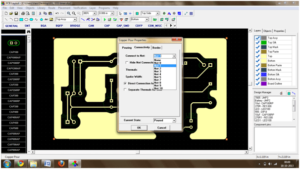
Screenshot of selecting a net on Diptrace

Fig. 28: Screenshot of selecting a net on Diptrace

After doing that setting the layout would be like that.
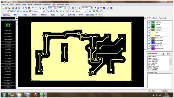
Screenshot of final layout on Diptrace

Fig. 29: Screenshot of final layout on Diptrace 

How to print layout

After completing the layout we can give this layout for printing. For this click on file menu, then click on preview  button.

Screenshot of print option in Diptrace

Fig. 30: Screenshot of print option in Diptrace

Bottom view.
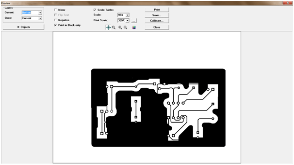
Screenshot of print preview of bottom side of layout

Fig. 31: Screenshot of print preview of bottom side of layout

Screenshot of print preview of bottom side of layout

Fig. 32: Screenshot of print preview of bottom side of layout

Top view

Screenshot of print preview of top side of layout

Fig. 33: Screenshot of print preview of top side of layout


Filed Under: Electronic Projects
Tagged With: Diptrace, pcb, pcb designing
 

Next Article

← Previous Article
Next Article →

Questions related to this article?
👉Ask and discuss on EDAboard.com and Electro-Tech-Online.com forums.


Tell Us What You Think!! Cancel reply

You must be logged in to post a comment.

EE TECH TOOLBOX

“ee
Tech Toolbox: 5G Technology
This Tech Toolbox covers the basics of 5G technology plus a story about how engineers designed and built a prototype DSL router mostly from old cellphone parts. Download this first 5G/wired/wireless communications Tech Toolbox to learn more!

EE Learning Center

EE Learning Center
“engineers
EXPAND YOUR KNOWLEDGE AND STAY CONNECTED
Get the latest info on technologies, tools and strategies for EE professionals.

HAVE A QUESTION?

Have a technical question about an article or other engineering questions? Check out our engineering forums EDABoard.com and Electro-Tech-Online.com where you can get those questions asked and answered by your peers!


RSS EDABOARD.com Discussions

  • Innovus Scan Reorder deletes Scan In Pad
  • How to get 3D model of ACPL-847-300E
  • is there vay for credit card size phone charger?
  • How to find the resonance frequency and impedance of a planar spiral coil in HFSS?
  • Why so few Phase shift full bridge controllers?

RSS Electro-Tech-Online.com Discussions

  • Can I make two inputs from one??
  • The Analog Gods Hate Me
  • How to make string LEDs?
  • Fixing board, Easy question HEX SCHMITT
  • It's Amazing What A Buck And A Quarter....

Featured – LoRa/LoRaWan Series

  • What is the LoRaWAN network and how does it work?
  • Understanding LoRa architecture: nodes, gateways, and servers
  • Revolutionizing RF: LoRa applications and advantages
  • How to build a LoRa gateway using Raspberry Pi
  • How LoRa enables long-range communication
  • How communication works between two LoRa end-node devices

Recent Articles

  • How to monitor temperature and humidity on a TFT display with graphics
  • Tria modules integrate edge AI processing with multi-core processors
  • pSemi introduces RF switch with 52 dBm PMAX,PEAK and 90-dBm IIP3 linearity
  • XP Power launches 1.3 kW power supply with 58.9 W/cm³ density
  • How to enable Wi-Fi provisioning in ESP32-based IoT products

EE ENGINEERING TRAINING DAYS

engineering

Submit a Guest Post

submit a guest post
Engineers Garage
  • Analog IC TIps
  • Connector Tips
  • Battery Power Tips
  • DesignFast
  • EDABoard Forums
  • EE World Online
  • Electro-Tech-Online Forums
  • EV Engineering
  • Microcontroller Tips
  • Power Electronic Tips
  • Sensor Tips
  • Test and Measurement Tips
  • 5G Technology World
  • Subscribe to our newsletter
  • About Us
  • Contact Us
  • Advertise

Copyright © 2025 WTWH Media LLC. All Rights Reserved. The material on this site may not be reproduced, distributed, transmitted, cached or otherwise used, except with the prior written permission of WTWH Media
Privacy Policy

Search Engineers Garage

  • Electronic Projects & Tutorials
    • Electronic Projects
      • Arduino Projects
      • AVR
      • Raspberry pi
      • ESP8266
      • BeagleBone
      • 8051 Microcontroller
      • ARM
      • PIC Microcontroller
      • STM32
    • Tutorials
      • Audio Electronics
      • Battery Management
      • Brainwave
      • Electric Vehicles
      • EMI/EMC/RFI
      • Hardware Filters
      • IoT tutorials
      • Power Tutorials
      • Python
      • Sensors
      • USB
      • VHDL
    • Circuit Design
    • Project Videos
    • Components
  • Articles
    • Tech Articles
    • Insight
    • Invention Stories
    • How to
    • What Is
  • News
    • Electronic Product News
    • Business News
    • Company/Start-up News
    • DIY Reviews
    • Guest Post
  • Forums
    • EDABoard.com
    • Electro-Tech-Online
    • EG Forum Archive
  • DigiKey Store
    • Cables, Wires
    • Connectors, Interconnect
    • Discrete
    • Electromechanical
    • Embedded Computers
    • Enclosures, Hardware, Office
    • Integrated Circuits (ICs)
    • Isolators
    • LED/Optoelectronics
    • Passive
    • Power, Circuit Protection
    • Programmers
    • RF, Wireless
    • Semiconductors
    • Sensors, Transducers
    • Test Products
    • Tools
  • Learn
    • eBooks/Tech Tips
    • Design Guides
    • Learning Center
    • Tech Toolboxes
    • Webinars & Digital Events
  • Resources
    • Digital Issues
    • EE Training Days
    • LEAP Awards
    • Podcasts
    • Webinars / Digital Events
    • White Papers
    • Engineering Diversity & Inclusion
    • DesignFast
  • Guest Post Guidelines
  • Advertise
  • Subscribe