PCB Design – Schematic Editing:
In PCB designing, the first step is Creating circuit or schematic capture. In this, we have to draw the schematic with necessary Electronic components. This step includes adding components, connections with wire, verifying the circuit, etc. To create a circuit in KiCad, we have to use Eeschema. It is powerful schematic capture software distributed as part of KiCad and is limited only by the available memory. Thus, there is no real limitation to the number of components, component pins, connections, or sheets. In the case of multi-sheet diagrams, the representation is hierarchical.
Before editing the circuit, we need to know some options and their functionalities.
| S.No | Name | Symbol | Description | Shortcut | ||
|---|---|---|---|---|---|---|
| 1 | Display Libraries |  |
|
– | ||
| 2 | Library Editor |  |
|
– | ||
| 3 | Annotate |  |
|
– | ||
| 4 | ERC |  |
|
– | ||
| 5 | Net List |  |
|
– | ||
| 6 | Generate BOM |  |
|
– | ||
| 7 | Edit footprints |  |
|
|||
| 8 | Pcb new |  |
|
– | ||
| 9 | Add components |  |
|
|
||
| 10 | Power symbol selector |  |
|
– | ||
| 11 | Draw a Wire |  |
|
|
||
| 12 | Draw a Bus |  |
|
|
||
| 13 | Draw Wire to Bus entry points | |
|
– | ||
| 14 | Draw bus to Wire entry points |  |
|
– | ||
| 15 | Not connected |  |
|
|
||
| 16 | Junction |  |
|
|
||
| 17 | Local Labels |  |
|
|
||
| 18 | Global Labels |  |
|
|
||
| 19 | Hierarchical Labels |  |
|
|
||
| 20 | Hierarchical Sheets |  |
|
|
||
| 21 | Import hierarchical labels |  |
|
– | ||
| 22 | Place hierarchical pin in sheet |  |
|
– | ||
| 23 | Graphical line |  |
|
|
||
| 24 | Textual comments |  |
|
|
||
| 25 | Delete |  |
|
|
Fig. 1: Screenshot of KICad Main Window
Note: Above table contains only some commonly used and important Eeschema options. I haven’t covered all of them. After knowing about these options, please refer to more shortcut keys, by selecting hotkeys option in the preferences menu. If any changes are needed, we can assign our own preferences also.
I am selecting a circuit from Engineersgarage.com, which consists of 8051 microcontroller, 16×2 LCD, ADC0804 and some other components.
Open the KiCad software and create a new project with a suitable name (Ex: EGtutorials).
Open KiCad > File menu > New project > Assign name and save it.
After creating the new project, we can see the project with sub files at the left side of the KICad main window.

Fig. 1: Screenshot of KICad Main Window
We can see that the saved folder has “.pro“ file extension and in sub-files “.sch ” file is schematic file (Eeschema).
Now we can start building the circuit. Open Eeschema and add components by selecting “Add components” option in the right toolbar. Or follow the steps.
Eeschema > Press “A” key> search component by typing its name > select component.
Ex: press “A” key and window will appear with libraries on screen. Many libraries are available like -74xx, -Atmel, – ADC-DAC etc. From these libraries, select the required component. If you want 16×2 LCD, then type name and search. If you find it, check it and add it to the worksheet. If not found, create 16×2 LCD using library editor. Repeat the same procedure unless all the required components are obtained.

Fig. 2: Screenshot of Choose Component Window in KIcad
In selected circuit, all that components are available except ADC0804. Actually, another series of ADC is available, but ADC0804 is not available. ADC0804 is 20 pin DIP IC. So, I am going to create it in the library editor.
Note: In the previous tutorial, I explained how to create a component in library editor. Please follow the same procedure here.
Steps to edit component:
1. Refer to the data sheet for pin diagram.
2. Open library editor > click on “create new component” > give the name as ADC0804.
3. Click on Place pin option > assign a name and number of the pin > select the Electrical type of the pin> click on “ok”.
4. Repeat the same procedure up to 20 pins. (precaution : be careful when selecting Electrical type of the pin)
5. Place Graphical rectangle that touches all the pins.
6. Save the component in the library folder.
7. Close the library editor > open the Add components > select ADC0804> place the component on worksheet.

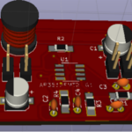
Fig. 3: Image showing Placement of a Components on PCB Layout
Now we have all the components. Place the components properly (as per convenience), and select “place wire” to connect components. I am connecting 16×2 LCD pins to microcontroller connections directly with the wire. To connect pins 1, 2, and 3 of LCD, we have to overlap some wires or else we have to connect using very long wires. So, in this case, I am using Nets and Local labels. (Please watch the video tutorial to understand better). In the same way, I am connecting potentiometers also. Pot has three pins; one pin is connected to Vcc another pin to Ground and third (middle) pin to pin 2 of LCD. Similarly, one more pot is connected to pin 9 of ADC0804. In the same manner, I made capacitor and resistor circuits also. Use local labels to connect ADC connections (name the labels carefully). After finishing all connections, connect power supply using “Vcc” and “GND” local labels as well as global labels. If we need this supply, we can use it in other sheets as well. Also, place “not connected” “ ” at every not connected pin in the circuit.
Note: When connecting circuit use shortcut to move the component, to place labels, etc. it will save your time.
After completing all connections, edit the component values like resistor values, capacitor values, etc. and “annotate” the circuit. Annotating is nothing but assigning names to components, for example, if we use 10 resistors in our circuit, initially, every component has the same name like “R?” If we left these components with same names without assigning different names, we will definitely get confused in PCB editing. So, Annotating is very important, do not skip it.
Precautions:
1. When connecting the wire between components, observe and connect them properly. If it is not connected properly, we will get the Errors at ERC.
2. Assign names to the labels selectively.
3. When creating a new component, take care about the Electrical type of the pin.
You may also like:

Filed Under: Featured Contributions, Tutorials

Questions related to this article?
👉Ask and discuss on EDAboard.com and Electro-Tech-Online.com forums.
Tell Us What You Think!!
You must be logged in to post a comment.