[[wysiwyg_imageupload:3201:]]
Submitted By Mahendar from Anna University of Technology,Tiruchirappalli.
Abstract – This paper proposes a low power Linear Feedback Shift Register (LFSR) for Test Pattern Generation (TPG) technique with reducing power dissipation during testing. The correlations between the consecutive patterns are higher during normal mode during testing. The proposed approach uses the concept of reducing the transitions in the test pattern generated by conventional LFSR. The transition is reduced by increasing the correlation between the successive bits. The simulation result show that the interrupt controller benchmark circuit’s testing power is reduced by 46% with respect to the power consumed during the testing carried by conventional LFSR.
Keywords –LFSR, Optimization, Low power, Test Patterns
Introduction
The main challenging areas in VLSI are performance, cost, testing, area, reliability and power. The demand for portable computing devices and communications system are increasing rapidly. These applications require low power dissipation for VLSI circuits. The power dissipation during test mode is 200% more than in normal mode [1]. Hence it is important aspect to optimize power during testing. Power optimization is one of the main challenges.
There are various factors that affect the cost of chip like packaging, application, testing etc. In VLSI, according to thumb rule 5000 of the total integrated circuits cost is due to testing. During testing two key challenges are:
· Cost of testing that can’t be scaled.
· Engineering effort for generating test vectors increases as complexity of circuit increases.
Based on 1997 SIA data, the upper curve shows the fabrication cost of transistor and lower curve shows the testing cost of transistor. Figure 1 shows that the fabrication cost transistor decreases over the decades according to Moore’s law but the testing cost as constant. [2] 
There are main two sources of power dissipation in digital circuits; these are static and dynamic power dissipation. Static power dissipation is mainly due to leakage current and its contribution to total power dissipation is very small. Dynamic power dissipation is due to switching i.e. the power consumed due to short circuit current flow and charging of load capacitances is given by equation:
P=0.5VDD2E(SW)CL FCLk
Where Vdd is supply voltage, E(sw) is the average number of the main challenges. Output transitions per 1/fclk, fclk. Is the clock frequency and CL is the physical capacitance at the output of the gate. Dynamic power dissipation contributed to total power dissipation. From the above equation the dynamic power depends on three parameters: Supply voltage, Clock frequency, switching activity. To reduce the dynamic power dissipation by using first two parameter only at the expense of circuit performance. But power reduction using the switching activity doesn’t degrade the performance of the circuit.
- Patterns can be very low. This can cause large to test large circuit, circuits are partitioned to save the test time but these parallel testing results in excessive energy and power dissipation. Due to the lack of at-speed equipment availability, delay is introduced in the circuit during testing. This cause power dissipation.
- In the successive functional input vectors applied to a given circuits in normal mode have a significant correlation, while the correlation between consecutive test switching activity its normal operation. Power dissipation in CMOS circuits is proportional to switching activity; this excessive activity during test may be responsible for cost, reliability, performance verification, and autonomy and technology related problems.
During testing large power is dissipated than in the normal mode. This is due to lack of correlation between theSuccessive test patterns generated by ATPG (for external testing) or LFST (for BIST) and this large power dissipation cases following effects:
- The increased power may be responsible for cost, reliability, performance verification, autonomy and technology related problems. Low power dissipation during test application is thus becoming an equally important figure of merit in today‘s VLSI circuits design and is expected to become one of the major objectives in the near future.
- High power and ground noise caused by high switching during testing are serious problem where the supply connects are poor. The excessive noise can change the logic state of the circuit lines leading good dies to fail the test and hence loss of yield.
- As the circuit is designed in the deep sub micron (DSM) technology, this uses small supply voltages and hence this reduces the use of special cooling equipment to remove the excessive heat during test. Low power testing is done at at-speed. But in other testing techniques, circuits are added to lower the frequency of circuit during test.
For complex circuits, hierarchical approach is used. The advantage of hierarchical approach is that every block is tested separately. Test input is given to each block and output is observed and verified. DFT (Design For Testability) is the action of placing features in a chip design process to enhance the ability to generate vectors, achieve a measured quality level or reduce cost of testing. The conventional DFT approaches use scan and BIST.
In this paper a modified low power LFSR are used in which the number of transitions of test pattern are reduced testing. The remainder paper is organized as follows: Section 2 describes the previous work while section 3 presents the proposed work. Section 4 describes the simulation results and conclusions.
PRIORWORK
There has been various low power approaches proposed to solve the problem of power dissipation during the testing. Some of the earliest work that has been proposed for optimizing the power during testing is discussed in this section of the paper. One method is to use Random Single Input Change (RSIC) test generation, which is used to generate low power test pattern. In this method, power consumption is reduced but at the additional cost isbetween 19% and 13% Another technique was proposed in [5]. This approach. This approach proposed a low transition LFSR for BIST applications. This reduces the average and peak power of circuit during testing. In [6] approach, a fault model and ATPG algorithm is chosen first and then test pattern are generated to obtain the desired fault coverage. There are various advantages of test pattern generation at a higher level than the gate level. WhileF. Corno et al has proposed for the low power test pattern generation for sequential circuit [7]. In this paper, redundancy is introduced during testing and this reduces the power consumption without affecting the fault coverage. In [8], it is shown that different LFSR architecture affects the power consumed and the hardware used. Jinkyu Lee et al [9] developed a LFSR reseeding scheme. In this approach, there are two goals, first is to reduce the number of transition in scan chain. Second is to reduce is the number of specified bits generated by LFSR reseeding.
BIST ARCHITECTURE
It is very important to choose the proper LFSR architecture consumes different power even for same polynomial. Another .Problem associated with choosing LFSR is LFSR design issue, which includes LFSR partitioning, in this the LFSR are differentiated on the basis of the basis of hardware cost and testing time cost.
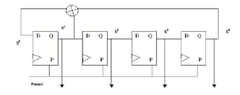
A typical BIST architecture consists of a test pattern generator (TPG), usually implemented as a linear feedback shift register (LFSR), a test response analyzer (TRA), implemented as a multiple input shift register (MISR), and a BIST control unit (BCU), all implemented on the chip (Figure 1). This approach allows applying at-speed tests and eliminates the need for an external tester. The BIST architecture components are given below
Circuit under Test (CUT): It is the portion of the circuit tested in BIST mode. It can be sequential, combinational or a memory. Their Primary Input (PI) and Primary output (PO) delimit it. Test pattern Generator
- (TPG): It generates the test patterns for CUT. It is a dedicated circuit or a microprocessor. The patterns may be generated in pseudorandom or deterministically.

· Multiple input signatures registers (MISR): it is designed for signature analysis, which is a technique for data compression. MISR efficiently map different input streams to different signatures with every small probability of alias. MISR are frequently implemented in built-in-self-test (BIST) designs, in which output responses are compressed by MISR.
· Test Response Analysis (TRA): It analyses the value sequence on PO and compares it with the expected output BIST Controller Unit (BCU): It controls the test execution; it manages the TPG, TRA and reconfigures the CUT and the multiplexer. It is activated by the Normal/Test signal and generates a Go/No go.
ALOGORITHM FOR LOW POWER LFSR
As discussed in the previous section LFSR is used to generate test patterns for BIST. In this, test patterns are generated externally by LFSR, which is inexpensive and high speed LFSR is a circuit consists of flip-flops in series. LFSR is shift register where output bit is an XOR function of input bits. The initial value of LFSR is called seed value. LFSR’s seed value has a significant effect on energy consumption. [3]. The output that influence the input are Called tap. A LFSR is represented by as polynomial, which is also known as characteristic polynomial used to determine the feedback taps, which determine the length of random pattern generation. The output of LFSR is combination of I’s and O’s. A common clock signal is applied to all flip-flops, which enable the propagation of logical values from input to output of flip-flops. Increasing the correlation between bits reduces the power dissipation. This can be achieved by adding more number of test vectors, which decreases the switching activity. LFSR is characterized by the polynomial by its characteristics polynomial and inverse of characteristics polynomial is generated polynomial.
In this approach the 3 intermediate test vectors are generated between every two successive vectors (say TI, T2). The total number of signal transition occurs between these 5 vectors are equivalent to the number of transition occurs between the 2 vectors. Hence the power consumption is reduced. Additional circuit is used for few logic gates in order to generate 3 intermediate vectors. The 3 intermediate vectors (Ta, Tb, Tc) are achieved bydown includes logic circuit design for propagation either the present or next state of flip-flop to second level of hierarchy. Second level of hierarchy is implementing Multiplexed (MUX) function i.e. selecting two states to propagate to output as shown in flow: 
The EDA tool is used in which conventional and low power LFSR is coded in Verilog hardware descriptive language and a seed value is given (010010100101101011010010100101101011) to the polynomial and primitive value polynomial in LFSR block. The outputs of the 36-bit LFSR are used as the inputs to the c42 ISVAS-85 a benchmark circuit of interrupt controller. In this c432 is used as CUT; the generated code is synthesized in Xilinx Web Pack 9.1 for Spartan 2e device. The hardware summary is obtained for each method implementation log file of Xilinx 9.1 project navigator. The RTL view of LP-LFSR with c432 benchmark circuit is shown in figure 5. 
V.RESULTS AND CONCLUSION
The results obtained from the Xilinx 9.1 implementation with the device xc3s200-4pq208 in which, we have generated VCD file after the post simulation. Xpower is used to calculate the with the simulation file. Results are obtained for each case and comparison of power dissipation is made on the basis of reports is give in table 1 and shown in figure 6.
|
TABLE.1 POWER DISSIPATION CONVENTIONAL AND LOW POWERM LFSR
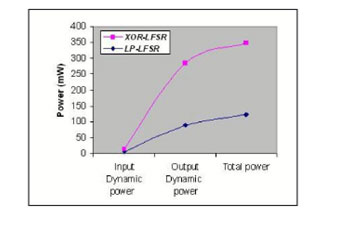
It is observed that the total power consumed in modified LFSR is 46% less than the power consumed with normal LFSR and output dynamic power is decreased by 44.6 %. It is concluded that low power LFSR is very useful for BIST Implementation in which the CUT may be Combinational, sequential and memory circuits. Using low power LFSR technique we can further decrease the power in BIST implementation.
Project Datasheet
Filed Under: Electronic Projects

Questions related to this article?
👉Ask and discuss on Electro-Tech-Online.com and EDAboard.com forums.
Tell Us What You Think!!
You must be logged in to post a comment.