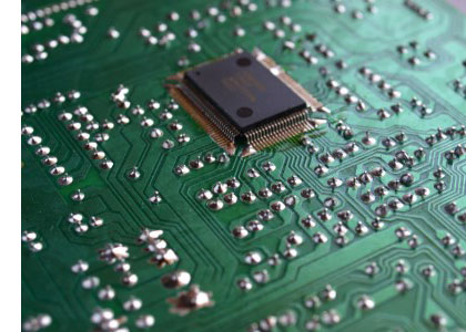
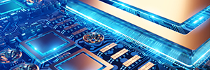
Fig. 1: A Represenational Image of Printed Circuit Board
The success of any creation is often dependent on the foundations it is built upon, be it the strength of a character, depth of a building’s foundations or the extent of a tree’s roots. Much in the same way, the success of any electronic device depends on what it is built on. The motherboard of any electronics device serves as a playground and a host to every form of electrical signal that performs some function for the equipment. Be it the communication signal between the North Bridge and processor on a computer, or a simple on-off signal in a routine school project, the effectiveness of the design is a function of the capabilities offered by the base board itself.
A Printed Circuit Board doesn’t just connect electrical components using etched copper pathways, but also provides mechanical strength to it. Printed Circuit Boards, or more appropriately, Printed Wiring Boards are found in almost all of the commercial products as a packaging medium as building blocks.
PCBs are a composite of organic and/or inorganic dielectric materials with many layers with wiring interconnects and also house components like inductors and capacitors. There isn’t any standard printing board as such and each board is unique, often a function of the product itself. There are industry standards for almost every aspect of PCB design, controlled by IPC, for example the IPC-2221, ‘Generic Standard on Printed Board Design’.
History
PCBs have evolved from the electrical connection systems developed in the 1850s. The first patents on Printed Wires were issued in 1903. Albert Hanson explained a layered structure of foil conductors laminated to insulation boards. Arthur Berry patented a ‘Print-and-Etch’ method in 1913 and Max Schoop patented Flame Spraying metal onto a board via a mask. Thomas Edison had experimented with chemicals for plating conductors on linen paper way back in 1904, but the method of electroplating circuit patterns was finally successfully patented to Charles Durcase in the year 1927. Charles Ducas had earlier patented a technique of creating electrical paths directly using stencils and electrically conductive ink in 1925.
World War II saw the invention of circuit boards that could withstand gunshots. But, the credit of developing the first PCB is given to Paul Eisler in 1943, for developing a method of etching conductive circuits on copper foil bonded to a non-conductive base reinforced by glass. The method remained dormant until late 50s when the transistors were introduced for commercial use. The presence of wire leads on electronic components led to the development of ‘Through Hole’ technology where holes were drilled into the PCB and the components soldered on to the board at those points. It was patented by a U.S. firm Hazeltyne in 1961. However, this process being slightly expensive and wasteful as the extra wire is cut off and not used much. Nowadays, ‘surface mount’ technology is gaining impetus as the demand for smaller, high density circuits is increasing.
Types of PCB
A PCB can be of four types: rigid boards, flexible and rigid-flex boards, metal-core boards and injection molded boards out of which the rigid board is the most popular. Further these may be single sided, double sided or multilayered. The mechanical, electrical, chemical and thermal properties of the material should be considered while making PCBs otherwise the reliability of the board suffers. Presently, copper-clad laminates of different reinforced resin systems are used in rigid boards. Examples include Fire resistant FR-4 epoxies, PTFE, cyanate esters, ployimides etc. Most commonly used reinforcement material is continuous filament E-Glass. Flexible and rigid flex-boards have random arrangements of conductors on a flexible base and may be with/without cover layers. Here, the wiring is restricted to select areas of the plane. In case of constraining metal core technology, the PCB can be of standard materials but the core materials must have low Coefficient of Thermal Expansion and strength to constrain the PCB. Copper-Invar-Copper and Copper-Molybdenum-Copper are two popular materials for this purpose. Molded boards have resins containing fillers which are molded into a die to form the required shapes.
Before anything is drawn onto the PCB, it first has to be designed and verified by means of simulation. The design process is hierarchical in nature and may follow either one of the two approaches:
1. Top-Down Design. 2. Bottom-Up Design
Top-Down Design
Top-Down Design: Designers start with a higher abstraction layer and work on its general functionality before creating a lower level building block for that layer. This creates organized designs as the overall structure is drawn first and complexity is tackled at a later, lower stage. It is like manufacturing a car body first and then making custom parts for it. 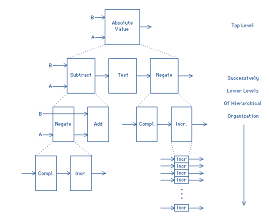

Fig. 2: Diagram explaining top down hierarchy of PCB design
Bottom-Up Design
Bottom-Up Design: In this methodology, designers first develop the smallest block and then go on to designing bigger blocks from smaller building blocks. This gives the design a modular approach and increases reusability of segments of design. This approach is like the manufacturing of a standard car in a factory, make the parts first and then put them into a single piece. 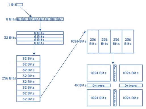

Fig. 3: Diagram Showing Bottom up Hierarchy of PCB Design
No matter what approach a designer chooses, the PCB has to meet certain signal-integrity requirements like crosstalk, SSO, noise, delay and reflections, electromagnetic compatibility, EMI specifications and susceptibility requirements, thermal requirements, strength etc. Designing the PCB is a part of a much wider design process. The netlist generation is an important step not just for PCB designers but for circuit simulation too. Netlist contains a net, or a complete set of interconnections and components used. Once the circuit simulation is successful, PCB designers get down to working out the most simple and efficient circuit pattern or artwork. By placing the components on the board in the software, the size of the board may be known. There are various automated component placement software which can speed the work of the designer and have different algorithms working on their back end. However, a seasoned designer would know that such software cannot always give satisfactory results and orderly placed components design is seldom the suitable design. The last step involves the placement of interconnect traces. This again can be an automated step using software based on popular algorithms like Lee algorithm, Hightower router, pattern router, channel router and gridless routers, but designer discretion is required. Once this step is completed, the board’s integrity is verified by subjecting the trace pattern to Design Rule Checks which check if all the tracks, vias and pads have been placed according to the design rule sets or not. The length of interconnects can lead to severe signal distortions. Hence, Signal-integrity, EMI compliance and other checks are performed as the next step.
PCB Manufacturing
Artwork is generated by sending the design files in a particular format to plotters and transparencies for PCB manufacturing are produced. After this the manufacturing of the PCB commences. There are mainly five standard technologies used in PCB manufacturing:
1. Machining: This includes drilling, punching holes and routing on a PCB with standard existent machinery and also new technologies like laser and water jet cutting. The strength of the board needs to be taken into account while machining for accurate hole diameters. Small holes make this method costly and less reliable due to reduced aspect ratio and also making plating difficult.
2. Imaging: This step transfers the circuit artwork onto individual layers. Single sided or double sided PCBs may use simple Screen Printing technology for creating the patterns on a print-and-etch basis. But this has a limitation on the minimum line width achievable. For fine line boards and multilayer boards, Photoimaging is used which may be applied by flood screen printing, dip coating, Electrophoresis, roller laminating or liquid roller coating. Recently, direct laser imaging and liquid crystal light valve imaging have also been employed for the same.
3. Laminating: This process is mainly used for manufacturing multilayer boards, or the base laminates of single/double sided boards. B-stage epoxy resin impregnated glass sheets are pressed between layers using hydraulic press to bond the layers together. The pressing may be cold, hot, vacuum assisted or vacuum autoclave nominated offering close control on dielectrics and thickness.
4. Plating: It is basically the metallization process which may be brought about either by wet chemical processes like electroless plating and electrolytic plating or dry processes like sputtering and CVD. While electroless plating offers high aspect ratios and no external current thus forming the core of additive technology, electrolytic plating is the preferred method for bulk metallization. Recent developments like the plasma processing offer greater efficiency and quality while taxing less on the environment.
5. Etching: The removal of unwanted metal and dielectric from the board takes place by either dry or wet processes. The uniformity of etching is the prime concern in this stage and to extend the fine line etching capabilities, new anisotropic etching solutions are being developed.
Design Flow
Design Flow
The overall design flow can be summarized in the flowchart as shown below: 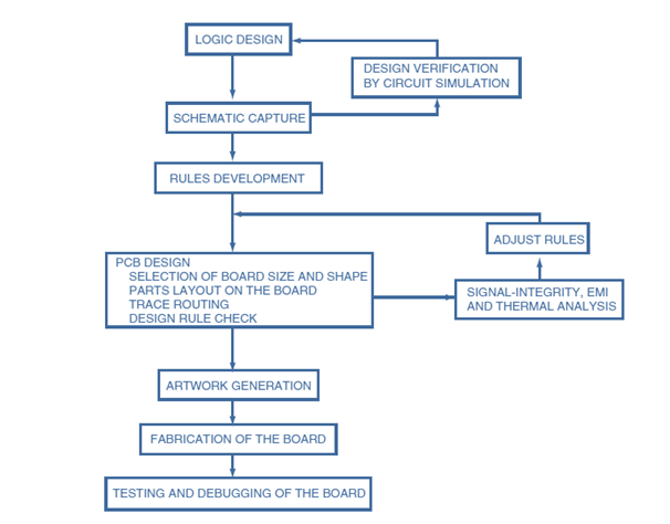

Fig. 4: Diagram Displaying PCB Design Flow
Throughout the manufacturing process of a PCB, visual and electrical inspection is carried out to locate any flaws that might have crept in due to process automation like ‘Tombstone effect’ when the solder is heated too quickly and one end of the component lifts up from the board failing to make contact, or excess flow of solder or bridging. Even after the manufacturing process, the boards are tested for the output levels under varying conditions of environment, stress and strain.
Back in the olden days, when PCBs had just been introduced, military was the chief consumer. But as the technology progressed and as the need grew, more and more interest was diverted towards better PCBs and as of today, they serve as the base for a multitude of components, gadgets and devices ranging from ever innovating computers and cell phones to basic equipments like television, radio and toys for children. Soon there are going to be more mobile phones than there are people in this world and the trend will continue to rise. This might be a convenience to the users, but isn’t without hazards either, combating which offers great scope for people from diverse fields.
Challenges
Risks & Challenges
Solder contains lead, which is a toxic material. On heating Solder, lead fumes are formed which should not be inhaled. However, it is necessary for performance reasons that such operations be done in closed areas. Proper processing and filtering of the fumes is required before they are allowed to enter the earth’s atmosphere. Due to rapidly changing technology, devices become outdated and obsolete in a matter of few months and sometimes even weeks, and as progressive population goes on embracing newer technology, the pile of older devices continues to get bigger day by day. It would be disastrous for the ecosystem if poisonous substances entered the system through these discarded materials, hence it causes disposal problems. Several mitigation procedures have been adopted by countries in order to tackle this situation like e-waste management, recycling electronic products, and salvaging parts from older equipment, reclaim and reuse of solder and buy back offers from the manufacturers. Development of cheap and non-toxic ways to make electrical connections like water soluble conductive molded plastics are being developed to replace wires and solder. Further, developments of technologies like three-dimensional molded plastic boards assure us of PCB technologies being a very dynamic field for many years to come.
Filed Under: Articles

Questions related to this article?
👉Ask and discuss on EDAboard.com and Electro-Tech-Online.com forums.
Tell Us What You Think!!
You must be logged in to post a comment.