It is responsibility of design engineer to get the most performance and capability out of the resources available in limited budget and that too for specific application requirements.
While the ideas presented here are around Atmel’s 89S52 microcontroller, these can be easily used with all other types of microcontrollers without any changes and configurations. This note discusses two such techniques to save microcontroller IO lines.
Interfacing 3×2 Keys
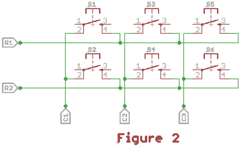
Fig. 1: Circuit Diagram of 3X2 Keypad
Usually in order interface 3×2 keys i.e. 6 keys, we will need six IO pins of microcontroller to take inputs. The basic schematic is shown in figure 1.
However, in regular practice we usually recommend using matrix scanning method to interface more keys where keys are arranged in row-column format and then can be scanned one by one. In such case, we will need 3 rows and 2 columns (or vice versa) to interface 3×2 keys as shown in figure 2. That means 5 IO pins are still required for interfacing.
Here is the third novel technique to reduce required IO pins further. This technique needs some additional (yet cheaper) hardware though. As shown in

Fig. 2: Circuit Diagram of 3X2 Keypad
schematic Figure 3, keys are connected in set of three keys each.
Each set has small signal switching diode connected in series (typical component recommended is 1N4148). Note the direction of diodes in each set as it is reversed in one set as against another.
In order to identify which key has been pressed; specific algorithm needs to be deployed as explained here. First pin P0 should be set to logic HIGH while P1 and P2 to logic LOW. Then after fractional delay, read input status at P1 and P2. If P1 is found HIGH, this means the path, P0-B2-D2-P1 is complete i.e. button B2 has been pressed. However, if P2 is found HIGH, that would mean P0-D5-B5-P2 is complete i.e. button B5 is pressed. Similarly, when P1 is set to HIGH keeping P0 and P2 LOW; B1 and B4 can be identified. Buttons B3 and B6 can be detected by setting P2 to HIGH and reading status of P0 and P1 respectively. Table 1 shows logical combinations for above mentioned algorithm to be used alongwith the circuit as per figure 3.
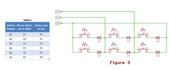
Fig. 3: Circuit Diagram of Keypad Interfacing with 8051 Microcontroller
Here the only hardware addition is of six small signal diodes which would not be a cost burdon on the design yet help in saving 2 to 4 IO pins.
Using Multiplexer for GPIO
Using Multiplexer for GPIO
How many times it happens that you are using low cost microcontroller and yet want to increase its outputs beyond specifications ? Typically, this would happen with special purpose signals such as serial port (Rx-Tx), SPI, I2C or even sensor inputs or for certain general purpose IOs.
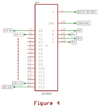
Fig. 4: Circuit Diagram of CD4067 Multiplexer
In case of certain microcontrollers where ADC is inbuilt, there are still limitations on no. of input channels such as 8 or less. What if you have more than 8 sensors to take inputs ? This is especially critical, when IOs are analog in nature rather than simple digital ones.
Here comes another novel technique of multiplexing using well known analog-digital multiplexer CD4067 IC. This IC is basically a digitally controlled bi-directional analog switch with very low impedance and low leakage current during OFF condition. It is 16 channel multiplexer with 4 binary control inputs and one enable pin. The IC is available in both DIP as well as SMD version. Figure 4 shows schematic circuit where only 5 pins are used to control one digital / analog IO of microcontroller with 16 channels. The IC simply acts as a single pole 16 way rotary switch and connects selected channel to common in/out pin X.
As shown in the schematic, P0-P3 are digital pins of microcontroller which provide binary address (0000 to 1111) for channel selection of multiplexer. CH-0 to CH-15 are sixteen channels which can act as input or output or both – independently. INH is control pin for IC which when set to LOW will disable all the channel connections and go into high-impedance state. Control pin can also be permanently grounded if not to be used for control signal. This will keep the multiplexer in enable condition all the time.
When P0-P3 are set to say 0101 i.e. binary equivalent of 5, channel CH-5 gets selected and thus pin 4 of IC is internally connected to pin 1. This connection has lower impedance which is typically about 115 ohms at 5 volts.
Figure 5 shows typical application circuit built around 89S52 where only 4 channels of CD4067 are used for reading data from four serial devices’ via their Tx signal (device Tx connected to Microcontroller’s Rx).
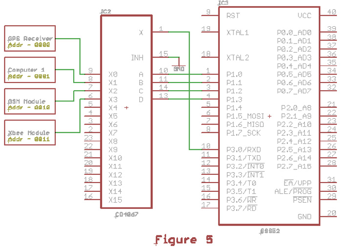
Fig. 5: Circuit Diagram of CD4067 Multiplexer interfacing with 8051 Microcontroller
As shown in circuit diagram, when MCU has to read data from computer, P1 output is set to 0001 such that ABCD becomes 0001 and channel 1 is connected to data pin X and so to P3.0. MCU then can read data from PC. When data is to be read from GSM module, simply set P1 = 0010 and for GSM module set it to P1 = 0000. The only drawback of this arrangement is that all channels can not be read simultaneously but one by one. For above mentioned application you can use two such ICs ; one for Rx signal and another for Tx signal.
Here you can replace 89S52 with AVR series microcontrollers and the single ADC pin can be used to read from 16 different analog sensors controlled in above mentioned fashion.
So, next time when you fall short of IO pins for interfacing devices, try to use these techniques and save a few pins; or what more, use analog multiplexing and expand the port connectivity almost by 16 fold.
Filed Under: Tutorials


Questions related to this article?
👉Ask and discuss on Electro-Tech-Online.com and EDAboard.com forums.
Tell Us What You Think!!
You must be logged in to post a comment.