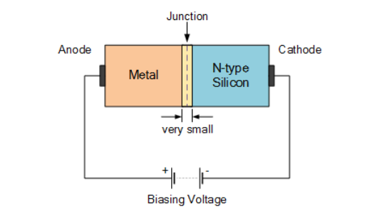
A diode is a two-terminal device that acts as a one-way switch. The Schottky is a metal-semiconductor diode known for very low forward voltage in which the metal forms the anode and the n-type semiconductor acts as the cathode.
The diode is named after German physicist Walter H. Schottky. It is also called Schottky barrier diode, surface barrier diode, low voltage diode, hot-electron diode, majority carrier diode, and hot-carrier diode. The most striking feature of a Schottky diode is its low forward voltage ranging from 150 mV to 450 mV. A low forward voltage makes Schottky diode a very high-speed switching device.
Construction of Schottky diode
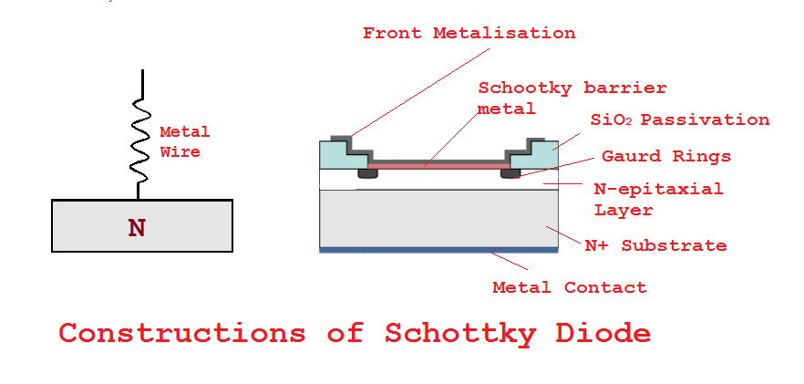
A Schottky diode is constructed by joining a metal electrode with a lightly-doped, n-type semiconductor. Due to the metal-semiconductor junction, a Schottky diode has no depletion region. The n-type material must be lightly doped; otherwise, the device will fail to operate as a rectifier. In a Schottky diode, the current flows due to majority charge carriers, i.e., electrons when forward biased. In reverse bias, the conduction of reverse saturation current immediately stops as there are no minority charge carriers, i.e., holes in a Schottky diode construction.
The most straightforward construction of a Schottky diode is a point contact between a metal wire with a lightly-doped n-type semiconductor material. This type of construction is simple but not much reliable. Another common manufacturing technique is using the vacuum to deposit metal onto n-type semiconductor material. First of all, the semiconductor surface is protected by an oxide ring. Then, the metal is deposited onto the semiconductor surface using a vacuum technique. The oxide ring avoids breaking the metal surface from the semiconductor due to electric fields established in reverse bias conditions. The most common metal used in the construction of Schottky diodes is Silicide. The Silicide is known to have very low ohmic resistance, which makes it the most preferred metal for Schottky diodes. Other metals that may be used in constructing the Schottky diode are aluminum and platinum. The selection of the metal and doping level of the n-type material plays an essential role in determining the diode’s forward voltage.
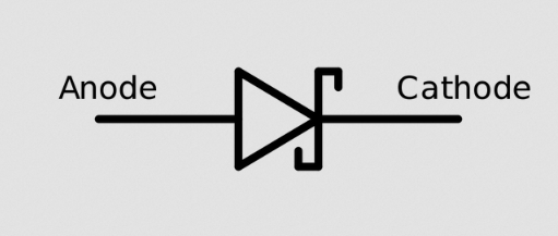
Symbol of Schottky diode
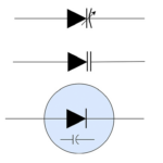
Schottky is a metal-semiconductor diode. It is represented by the following circuit symbol.
VI characteristics of Schottky diode
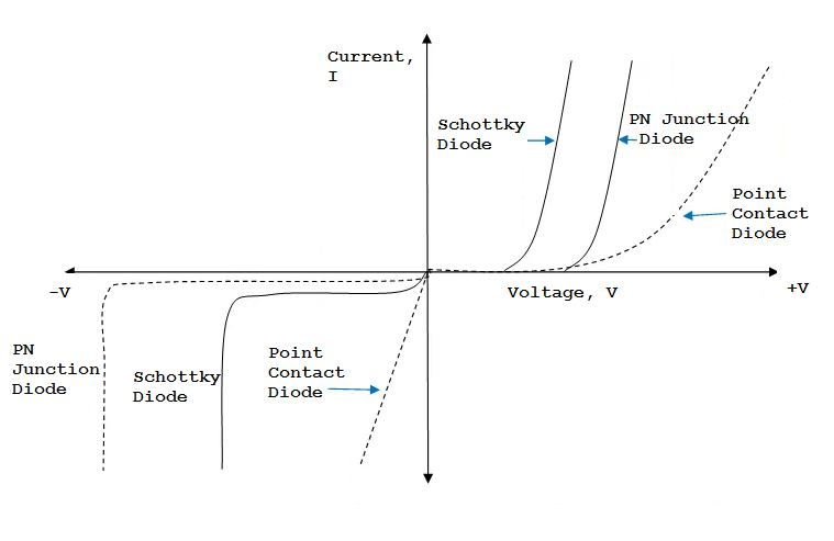
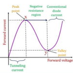
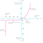
The voltage-current characteristics of a Schottky diode are shown in the graph below.
In forward conditions, you may notice that the knee voltage of the Schottky diode is less than the typical PN junction diode. The forward voltage of a typical PN junction diode ranges from 300 mV to 900 mV. In the case of the Schottky diode, the forward voltage ranges from 150 mV to 450 mV. Germanium diode has a forward voltage of 300 mV, but it is still not as fast as a Schottky diode. Secondly, the voltage-current curve of a PN junction diode is non-linear, showing an exponential rise in current beyond knee voltage. Due to metal-semiconductor junction in a Schottky diode, the VI curve in the forward bias region is somewhat linear. If the VI curve of a Schottky diode gets almost linear, then it is instead considered an ohmic metal-semiconductor contact.
In the reverse bias region, it can be seen that a Schottky diode conducts a much higher reverse saturation current. The reverse current in a Schottky diode is not due to minority charge carriers; instead, it only contributes to electron current. Again, it can be noticed that the reverse breakdown voltage of the Schottky diode is smaller than the PN junction diode.
Working of Schottky diode
A Schottky diode is basically a metal-semiconductor junction. A metal-semiconductor junction is considered a Schottky diode when it exhibits rectifying property. Such a junction is formed only when the n-type material is lightly doped. A junction formed with a heavily doped n-type semiconductor does not have a rectification feature and serves as an ohmic contact due to linear V-I characteristics. Although a metal-semiconductor junction virtually has no well-defined depletion region, it still has a potential barrier against majority charge carriers at the junction point. This is called the Schottky barrier. The height of the Schottky barrier is important. The metal-semiconductor junction performs rectification only when the Schottky barrier height is sufficient. A high Schottky barrier makes the voltage-current output non-linear.
The work functions, i.e., the energy required to free an electron from an ion, of n-type semiconductor and metal are different. Electrons in n-type semiconductors have more potential energy than free electrons in metal. The difference in metal and semiconductor work functions is equal to the Schottky barrier height, which opposes any movement of electrons from the semiconductor to the metal. As there is no P-type semiconductor in the Schottky diode, holes are not the majority charge carriers.
In unbiased conditions, when metal and semiconductor are joined, the electrons in n-type semiconductors move from n-type material to the metal side as they have higher potential energy. They leave behind positive ions at the semiconductor side of the junction. The metal already has plenty of free electrons. The electrons passed by the n-type material create negative ions at the metal side of the junction. This creates a potential barrier at the metal-semiconductor junction called the Schottky barrier. As the metal already has many free electrons, the impact of this potential barrier is seen on the semiconductor side only. The barrier opposes any further movement of electrons from n-type material towards the metal side. The transfer of electrons also bends the energy levels at the junction.
When the metal side (anode) is connected to the positive terminal and the semiconductor side (cathode) is connected to the negative side of a battery or voltage source, the diode is forward biased. The forward voltage increases the kinetic energy of the electrons in n-type material. However, these electrons cannot cross over to the metal side until they gain enough kinetic energy to overcome the Schottky barrier. When the forward voltage increases and electrons in n-type material gain kinetic energy higher than the Schottky barrier, the barrier is diminished. The current starts rising across the diode exponentially. As the Schottky barrier is tiny compared to the potential barrier in a typical PN junction diode, the current starts rising exponentially as soon the forward voltage is increased by 150~300 mV.
When the metal side (anode) is connected to the negative terminal and the semiconductor side (cathode) is connected to the positive side of a battery or voltage source, the diode is reverse biased. The reverse bias voltage increases the Schottky barrier, and few electrons can pass through the metal-semiconductor junction. A small amount of current flows through the diode due to free electrons in the metal side. The metal side has plenty of free electrons; the reverse current through a Schottky diode is higher than in a typical PN junction diode. As the reverse voltage increases, the Schottky diode also experiences Avalanche breakdown similar to a PN junction diode. Because the free electrons are higher on the metal side, the breakdown is achieved at a smaller reverse voltage than a typical PN junction diode.
It should be noted that the Schottky diode is a unipolar device, while the PN junction diode is a bipolar device. The current flow across a Schottky diode is only due to electrons. While in a PN junction diode, the current flow through the diode is due to electrons and holes. The holes are entirely absent in a Schottky diode.
Specifications of Schottky diode
The following specifications are worth noting in the datasheet of any Schottky diode.
- Forward voltage: This is the forward bias voltage at which the current through the diode starts rising exponentially. This is typically from 150 mV to 450 mV for all Schottky diodes.
- Capacitance: This is the diode capacitance exhibited by Schottky. It is in the picofarads range. In an equivalent model of Schottky diode, the capacitor must be replaced by the same capacitance value.
- Reverse leakage current: This is the typical reverse current value when reverse voltage is applied. It is specified for a given temperature. The reverse leakage current increases as the temperature rises.
- Reverse breakdown voltage: This is the peak inverse voltage at which the Schottky diode breakdowns in reverse bias.
- Reverse recovery time: The switching time required by the Schottky diode to transition between the states of ON and OFF. It is typically in pico-seconds or nano-seconds.
- Working temperature: The operating temperature that the metal-semiconductor junction can tolerate.
Schottky diode vs. PN junction diode
Schottky diode is a unipolar device whose current flow is entirely due to electrons. Many differences distinguish a Schottky diode from a typical PN junction diode (small-signal or rectifier diodes). The Schottky diode is constructed by joining metal with an n-type semiconductor, while the PN junction diode is constructed by joining P-type and N-type semiconductors. A PN junction diode is a bipolar device in which current flows due to electrons and holes. The forward knee voltage of the Schottky diode is much less than a PN junction diode and its reverse recovery time and reverse recovery loss are also shorter. This makes Schottky diode a high-speed switching device compared to a typical PN junction diode. That is why the diode used in logic circuit designs is usually Schottky.
Advantages of Schottky diode
Schottky diode offers many advantages compared to a PN junction diode. It has a very low turn-on voltage. The turn-on voltage of a typical PN junction diode is 300~900 mV, while the turn-on voltage of the Schottky diode is just 150~300 mV. The Schottky diode has virtually no depletion region, so it delivers a high current output even when a small-signal voltage is applied. Its junction capacitance is also lesser due to the same reason. As the current rises immediately on applying a small voltage, the heat dissipation or energy loss in a Schottky diode is very low. The Schottky diode has a minimal reverse recovery time due to the absence of any depletion region. Because Schottky diode has significant current output even for small bias voltage, it is comparatively noise-free. The Schottky diode pros make it a preferred choice for small-current and high-frequency applications.
Disadvantages of Schottky diode
The main disadvantage of Schottky diodes is their large reverse leakage current. They also break down at lower reverse voltage compared to typical semiconductor diodes. That is why Schottky diodes are only suitable for small-signal and high-frequency circuits.
Applications of Schottky diode
Some of the notable applications of the Schottky diode are the following.
General-purpose rectifiers: The fast switching operation in Schottky diodes makes them a suitable signal rectifier. Schottky diodes have high current density and low forward voltage drop. This minimizes the wastage of energy in a rectification circuit. Schottky diodes dissipate less heat, and so require smaller heat sinks. This reduces the overall cost and size of the rectifier circuit.
Solar cells: Schottky diodes are helpful for reverse voltage protection of solar cells. The low forward drop in Schottky diodes makes them energy efficient in a solar energy circuit.
Clamping: Schottky diodes are used as switching diodes in transistor clamping circuits. For clamping, the Schottky diode is connected between the collector and the base of the driver transistor. When turned ON, the Schottky diode delivers a high current at low bias voltage. Again as its reverse recovery time is much smaller, the switching time of the transistor is significantly improved. Schottky diodes have been used as clamping diodes in logic circuit ICs. These ICs have LS or S included in their circuit code names like 74LS or 74S.
Power OR circuits and SMPS: As Schottky diodes have a very low forward voltage, they are beneficial in circuits where two different power supplies drive the load like from the mains supply and a battery. That is why Schottky diodes are frequently used in SMPS and inverter circuits.
RF mixing and detection: High current density, high switching speed, low junction capacitance, and low forward voltage make Schottky diodes ideal for low-current high-frequency applications. Schottky diodes are frequently used in diode ring mixers and RF signal detectors.
It can be seen that Schottky diodes are suitable for both low-signal and high power applications. The specialty of the Schottky diodes is that they fit best to the opposite extremes of electronic applications.
Schottky diode examples
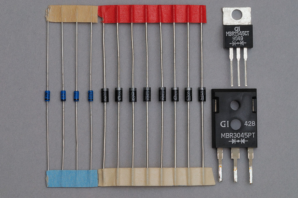
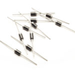
Hundreds of Schottky diode models are available from several manufacturers. Some notable examples of Schottky diodes include 1N5822, FR107, 1N4148W, 1N5711, FR207, BAT42, 1N5828, and 1N6263.
You may also like:
Filed Under: Featured, Tutorials, What Is


Questions related to this article?
👉Ask and discuss on Electro-Tech-Online.com and EDAboard.com forums.
Tell Us What You Think!!
You must be logged in to post a comment.