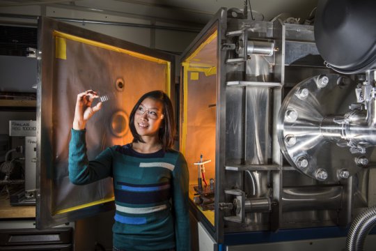
That splatting action is a core part of a Sandia National Laboratories project to lay down ceramic coatings kinetically. By making high-velocity submicron ceramic particles slam onto surfaces at the room temperature, Sarabol and her team members avoid the high temperatures otherwise needed to process ceramics such as barium and alumina titanate.
Layering at room temperature makes microelectronics design and engineering more flexible and could someday result in better, less costly microelectronics components that underpin modern technology. The kinetic process produces nanocrystalline layers that are highly strong and could be employed s protective coatings against wear, oxidation, corrosion, and the like.
Maintaining the particle kinetic energy through the bow shock layer is crucial to achieve material plastic deformation, and without plastic deformation there is no coating and no sticking. When a particle impacts the substrate or another layer, it plastically deforms and alters shape by a procedure known as dislocation nucleation and slip. Group of Sarabol discovered particles have nanofractures that make them “lay down onto a substrate like splatting cookie dough, preparing a pancake-shaped grain.”
The next substance that hits and deforms tamps down the original layer, preparing an even tighter bond. “So you have both the substances deformation and shape alter and fracturing without fragmentation and eventually the tamping from subsequent particles to help build the layer,” Sarabol says.
Those mechanisms make numerous layers possible, building up coatings that are tens of microns thick. “We have made nickel layers as thick as 40 microns, and in literature I’ve seen reports of up to about 80 microns for ceramics,” says Sarabol. Group members have successfully deposited numerous substances employing the method, including nickel, copper, aluminium oxide, barium titanate, carbide compounds, and titanium dioxide. Likely applications for such short list of substances alone comprise resistors, capacitors, inductors, electronic contacts and wear surfaces.
An exciting application particular to barium titanate films is electronic field management in high-voltage systems. High-voltage capacitors, for instance, are prone to failure where the dielectric substance meets the copper electrode and air, preparing a three-material junction.
“If you spray on barium titanate at this junction, you open up the possibility of high power capacitors,” says Sarabol. “There is a much more to do before we accomplish good enough properties for that.”
Other scientists are interested in electronic contacts, protective layering or consolidating brittle and intermetallic compounds for the first time.
Conclusion
The procedure also spans the microscale gap between two established technologies, sleek films and thermal spray technology. Thin films are coating layers, varying in size from nanometers to a few microns that can be defined into accurate electronic circuits and are patterned through photolithography methods instead of a conventional printed circuit boards. Thermal spray method can produce coatings beginning at about 50 microns up to a few centimetres. “This can bridge that missing gap, where you can begin to deposit hundreds of nanometres of substances up to a hundred microns,” says Sarabol
Filed Under: News

Questions related to this article?
👉Ask and discuss on EDAboard.com and Electro-Tech-Online.com forums.
Tell Us What You Think!!
You must be logged in to post a comment.