In the previous tutorials, all the circuits designed were combinational circuits. In combinational circuits, the binary output is dependant only on the current state of the inputs. So, actually, the combinational circuits have a static operation. They can have input from a fixed set of values for which the output is known to outcome in a defined range at any instant of time.
In practice, most of the electronic devices are dynamic in operation. They process a set of binary information received within a range of time at different instants to effectively output a real-time and relevant outcome. For this, the electronic devices contain memory elements to store digital information received at a previous instant of time and have the digital circuitry that can process information received at present instant as well as previous instant to output a relevant outcome. Like, a computer might need to keep results of previous computation for a next computation in line.
So, the type of digital circuits whose output not only depends on current state but also previous state of inputs are called sequential circuits. The sequential circuits are combinational circuits having feedback from memory elements. At any instant of time, the combinational circuitry within a sequential circuit takes present input and retrieves past input states from memory elements to perform computing. Once done with the computing, before the next computing to occur the combinational part of the sequential circuit stores the currently received input states to the memory elements. It can be said that the memory elements in a sequential circuit works as a feedback element. With memory elements at disposal, the sequential circuits are capable of storing, retaining and retrieving the previous state of inputs or say states of inputs in the previous instant of time.
There are two types of sequential circuits –
1) Synchronous Sequential Circuits
2) Asynchronous Sequential Circuits
The two types of sequential circuits differ in the timing scheme of their signals. The synchronous sequential circuits operate data on periodic clock signals, so they operate on binary data at discrete instants of time. The periodic clock signal is generated by a timing device called clock generator and the clock signal is generated and received as pulses. The computation of data by the combinational circuitry of the synchronous sequential circuit as well as storing and retrieving data from the memory elements is performed on the arrival of clock pulses i.e. when clock signal changes from 0 to 1 in such circuits. Meanwhile, the clock signal downs back to 0, the combinational circuitry of the synchronous circuit readies for the next cycle of computation while memory elements store the previous state of inputs and readies for the same to be retrieved on the arrival of the next pulse. For synchronous operation of combinational circuitry and memory elements according to the periodic clock signal, the propagation delay in the logic gates building the respective circuits are controlled accordingly. The rate at which the master clock generates the pulses must be slow enough to permit the slowest circuit to respond. This limits the speed of all circuits. It can be said that synchronous circuits are built by integrating together combinational circuitry, memory elements and clock generator. A synchronous sequential circuit can be represented by the following block diagram –
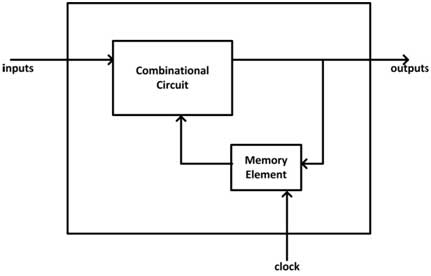
Fig. 1: Block Diagram of Synchronous Sequential Circuits
In asynchronous sequential circuits, the feedback of the previous states of input to the combinational circuitry can be at any instant of time instead of being periodic in nature and so, it depends on the order of input signals rather than occurrence of any clock pulse. In such circuits, the memory elements are coupled with time delay circuits, so that the feedback of the previous state of inputs can be received at the instant the present inputs are received. In most of the cases, the propagation delay through gates in memory elements is sufficient to produce the required time delay. In such circuits, the storage capability of the memory elements also depends on the signal propagation delay. The asynchronous circuits can be unstable or unreliable at times due to unprecedented time delays in circuitry or inputs to the circuit. Therefore, designing of asynchronous sequential circuits always need extra caution and technicalities. So, it can be said that asynchronous sequential circuit are built by integrating together combinational circuitry and memory elements with defined time delays in signal propagation.
Compared to combinational circuits, the sequential circuits are slower as they either have to synchronize according to clock signal in case of synchronous circuits or must have defined time delays in case of asynchronous circuits. The combinational circuits since only depend on present states of input, process the data immediately only affected by the propagation delay of signals through the gates.
However, sequential circuits incorporates the memory elements that are a vital part of any modern electronics. Most of the electronic devices need to store or retain data as need of the computation. The sequential circuits though being speed limited in their very design concept are the most abundant digital circuits in electronics.
Memory Elements –
The memory elements are essential in building any sequential circuit. The simplest memory element can store a single bit at any time. A group of such memory elements form larger memories. There are two types of single-bit storing memory elements – Latches and Flip-Flops. Both can store a single bit at a time.
The latches are level-sensitive memory elements that respond to either 0 or 1 state of the signal, while flip-flops are transition sensitive memory elements that respond to transition of signal from 0 to 1 and vice-versa. Being responsive to signal transitions, the flip-flops are called edge sensitive devices. The flip-flops themselves are constructed from latches. The latches are used as memory elements in asynchronous sequential circuits but they cannot be used in synchronous circuits. In synchronous circuits, the flip-flops are used as memory elements.
In a stable state, the output of a flip-flop remains either 1 or 0. The output of a flip-flop changes only when a clock pulse is received by it. The output of a flip-flop depends either on the present data input to it or the value currently stored in it or on both. The combinational circuitry of a synchronous circuit must be in sync with the clock pulses and reach a stable state before previous input states are passed to be stored in flip-flops. The circuit must be able to respond to the change in the states of flip-flops before the next clock pulse is arrived. So, the duration of clock pulse need to be pre-determined for proper functioning of a synchronous circuit. It must be noted that these memory elements – latches and flip-flops retain binary information until they are supplied power. In case, there is a power shutdown, the data retained by them at a moment is lost.
Latches –
Latches are level sensitive memory devices. They are used in asynchronous sequential circuits. They are also the building blocks of flip-flops. There are three types of latches –
1) SR Latch
2) S’R’ Latch
3) D Latch
SR Latch – The SR latch is built by two cross-coupled NOR gates. It has two inputs – set (S) and reset (R) while two outputs Q and Q’. The Q and Q’ are normally complement of each other. When the input set is 1 and input reset is 0, the output Q becomes 1 and Q’ becomes 0. When the input set is 0 and input reset is 1, the output Q becomes 0 and Q’ becomes 1. When both set and reset are 0, the SR flip-flop retains the output state i.e. if previously Q had become 1 and Q’ had become 0, the same states will be retained while both set and reset are 0. Similarly, if previously Q had become 0 and Q’ had become 1, the same states will be retained while both set and reset are 0. If both set and reset are 1, then both Q and Q’ becomes 0 which is forbidden. So, either of the set or reset being 1 changes the bit stored by the SR latch, if both becomes 0, the stored bit is retained while both being 1 is a forbidden condition. The SR latch can be built by NOR gates as follow –

Fig. 2: Logic Gate Diagram of SR Latch
The operation of an SR latch can be summarized by the following function table –

Fig. 3: Truth Table of SR Latch
S’R’ Latch – S’R’ latch is a type of SR latch which is built from two coupled NAND gates instead of two coupled NOR gates. In S’R’ latch when the input set is 1 and input reset is 0, the output Q becomes 0 and Q’ becomes 1. When the input set is 0 and input reset is 1, the output Q becomes 1 and Q’ becomes 0. When both set and reset are 1, the S’R’ flip-flop retains the output state i.e. if previously Q had become 0 and Q’ had become 1, the same states will be retained while both set and reset are 1. Similarly, if previously Q had become 1 and Q’ had become 0, the same states will be retained while both set and reset are 1. If both set and reset are 0, then both Q and Q’ becomes 1 which is forbidden. So, either of the set or reset being 0 changes the bit stored by the S’R’ latch, if both becomes 1, the stored bit is retained while both being 0 is a forbidden condition. It can be seen that the output of S’R’ latch is always complement of the output as in SR latch, so it got its name – S’R’ latch. The S’R’ latch can be built by NAND gates as follow –
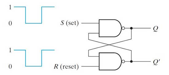
Fig. 4: Logic Gate Diagram of S’R’ Latch
The operation of an S’R’ latch can be summarized by the following function table –

Fig. 5: Truth Table of S’R’ Latch
The SR or S’R’ latch can have additional enable input to control the change in its state. The enable input can be added by connecting two additional NAND gates to the basic circuit of the SR latch as follow –

Fig. 6: Logic Gate Diagram of SR Latch with Enable Input
The SR latch with enable input has the following function table –

Fig. 7: Truth Table of SR Latch with Enable Input
D Latch – D Latch is a variant of SR latch or S’R’ latch to eliminate the forbidden condition of their function table. In a D Latch, there are only two inputs – Data (D) and Enable (En) and there are two outputs Q and Q’. The enable input can be either active low or active high. In case, enable input is active high, if there is a 0 at enable input the data is retained by the latch and not transferred to the outputs. When the enable input is set 1, if input data is 0, Q becomes 0 and Q’ becomes 1 while if input data is 1, Q becomes 1 and Q’ becomes 0. For active high enable input, the D latch has the following function table –

Fig. 8: Truth Table of Active High D Latch
If enable input is active low, the data is retained by the latch when enable input is set to 1 and transferred to the output when enable input is set to 0. The enable input can be made active low by connecting an inverter gate to it. With active low enable input, the D Latch has the following function table –

Fig. 9: Truth Table of Active Low D Latch
A D Latch is constructed by coupling input to NAND gates in an SR latch having Enable input. While coupling the NAND gates in first level of the logic gate implementation of the D Latch, the Data input is directly connected to Set (S) input of the SR latch while it is connected through an inverter to the Reset (R) input of the SR latch. This way, when Data (D) is 0, Set is 0 and Reset is 1 while when D is 1, Set is 1 and Reset is 0. A D latch has the following logic gate diagram –
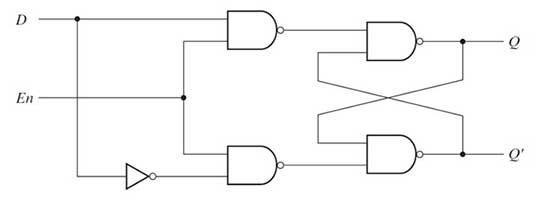
Fig. 10: Circuit Diagram of D Latch
Since in a D latch, the data is as it is transferred to the output Q when Enable (En) is set 1 in case of active high or is set 0 in case of active low configuration while it is retained in reverse state of the enable input, the D latch is also called transparent latch.
The latches are used as memory elements in asynchronous sequential circuits. In the next tutorial, Flip Flops and their different types will be discussed. The flips flops are the memory elements used in synchronous sequential circuits.
You may also like:
Filed Under: Digital Electronics, Tutorials




Questions related to this article?
👉Ask and discuss on Electro-Tech-Online.com and EDAboard.com forums.
Tell Us What You Think!!
You must be logged in to post a comment.