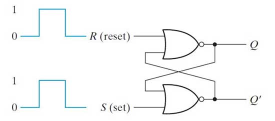
The operation of an SR latch can be summarized by the following function table –
|
S |
R |
Q |
Q’ |
Remark |
|
1 |
0 |
1 |
0 |
Bit set to 1 |
|
0 |
0 |
1 |
0 |
Bit retained |
|
0 |
1 |
0 |
1 |
Bit changed to 0 |
|
0 |
0 |
0 |
1 |
Bit retained |
|
1 |
1 |
0 |
0 |
Forbidden condition |
S’R’ Latch – S’R’ latch is a type of SR latch which is built from two coupled NAND gates instead of two coupled NOR gates. In S’R’ latch when the input set is 1 and input reset is 0, the output Q becomes 0 and Q’ becomes 1. When the input set is 0 and input reset is 1, the output Q becomes 1 and Q’ becomes 0. When both set and reset are 1, the S’R’ flip-flop retains the output state i.e. if previously Q had become 0 and Q’ had become 1, the same states will be retained while both set and reset are 1. Similarly, if previously Q had become 1 and Q’ had become 0, the same states will be retained while both set and reset are 1. If both set and reset are 0, then both Q and Q’ becomes 1 which is forbidden. So, either of the set or reset being 0 changes the bit stored by the S’R’ latch, if both becomes 1, the stored bit is retained while both being 0 is a forbidden condition. It can be seen that the output of S’R’ latch is always complement of the output as in SR latch, so it got its name – S’R’ latch. The S’R’ latch can be built by NAND gates as follow –

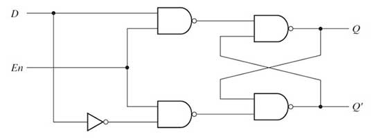
 Since in a D latch, the data is as it is transferred to the output Q when Enable (En) is set 1 in case of active high or is set 0 in case of active low configuration while it is retained in reverse state of the enable input, the D latch is also called transparent latch.
Project Source Code
###
//Program to###
Filed Under: Electronic Projects

Questions related to this article?
👉Ask and discuss on Electro-Tech-Online.com and EDAboard.com forums.
Tell Us What You Think!!
You must be logged in to post a comment.