
Fig. 1: An Image Of Switched Mode Power Supply
D.C. to D.C. converters and D.C. to A.C. Converters belong to the category of Switched Mode Power Supplies (SMPS). The various types of voltage regulators, used in Linear Power Supplies (LPS), fall in the category of dissipative regulator, as they have a voltage control element usually transistor or zener diode which dissipates power equal to the voltage difference between an unregulated input voltage and a fixed supply voltage multiplied by the current flowing through it. The switching regulator acts as a continuously variable power converter and hence its efficiency is negligibly affected by the voltage difference. Hence the switching regulator is also known as ‘non-dissipative regulator’. In a SMPS, the active device that provides regulation is always operated in cut-off or in saturation mode.
The input D.C. Supply is chopped at a higher frequency around 15 to 50 kHz using an active device like the BJT, power MOSFET or SCR and the converter transformer. Here the size of the ferrite core reduces inversely with the frequency. The lower limit is around 5 kHz for silent operation and an upper limit of 50 kHz to limit the losses in the choke and in active switching elements. The transformed wave form is rectified and filtered. A sample of the output voltage is used as the feedback signal for the drive circuit for the switching transistor to achieve regulation.

Fig. 2: Simple Block Diagram Of Switched Mode Power Supply
The oscillator in above figure allows the control element to be switched ON and OFF. The control element usually consists of a transistor switch, an inductor, and a diode. For each switch ON, energy is pumped into the magnetic field associated with the inductor which is a transformer winding in practice. This energy is then released to the load at the desired voltage level.
By varying the duty cycle or frequency of switching, we can vary the stored energy in each cycle and thus control the output voltage. Higher efficiency is obtained since only the energy required is pumped to maintain the load current hence no power dissipation.
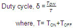

Fig. 3: Simple Circuit Diagram Of Switched Mode Power Supply
The major feature of SMPS is the elimination of physically massive power transformers and other power line magnetic. The net result is smaller, lighter package and reduced manufacturing cost, reducing primarily from the elimination of the 50 Hz components. The basic concept of switching regulator in a simple form is shown in this figure below.
Types of SMPS:
· D.C. to D.C. Converter:
· Forward Converter:
· Flyback Converter:
· Self-Oscillating Flyback Converter:
D.C. to D.C. Converter:
The block diagram of D.C. to D.C. converter (SMPS) is shown here. 
Fig. 4: Block Diagram Showing DC-DC Convertor SMPS
Here, the primary power received from AC main is rectified and filtered as high voltage DC. It is then switched at a huge rate of speed approximately 15 kHz to 50 kHz and fed to the primary side of the step-down transformer. The step-down transformer is only a fraction of the size of a comparable 50 Hz unit thus reliving the size and weight problems. The output at the secondary side of the transformer is rectified and filtered. Then it is sent to the output of the power supply. A sample of this output is sent back to the switch to control the output voltage.
SMPS rely on PWM to control the average value of the output voltage. The average value of the repetitive pulse waveform depends on the area under the waveform. As load increases, output voltage tends to fall. Most switching power supplies regulate their output using the method called Pulse – Width Modulation (PWM). The power switch which feeds the primary of the step-down transformer is driven by the PWM oscillator. When the duty cycle is at 50%, then the maximum amount of energy will be passed through the step-down transformer. As the duty cycle decreases the power transmitted is less hence low power dissipation.
The Pulse Width signal given to the switch is inversely proportional to the output voltage. The width or the ON time of the oscillator is controlled by the voltage feedback from the secondary of the rectifier output and forms a closed loop regulator. Since switching regulator is complex, modern IC packages like Motorola MC 3420/3520 or Silicon General SG 1524 can be used instead of discrete components.
Forward Converter
In a forward converter the choke carries both current both when the transistor is conducting as well as it is not. The diode carries the current during the OFF period of the transistor. Therefore, energy flows into the load during both the periods. The output voltage Vo can only be less than Vs in this circuit. The choke stores energy during the ON period and also passes some energy into the output load. The diode serves two functions.
1. It provides a discharge path for the choke so that, when the transistor switches opens, there is no arcing due to the induced high voltage.
2. It provides a path for the current in the coil to decay.

Fig. 5: Circuit Diagram Of SMPS Forward Converter

Fig. 6: Graph Showing Current And Voltage Waveforms Of Forward Converter
Type3: Flyback Converters
Flyback Converter:
In the flyback converter, the energy is stored entirely in the magnetic field of the inductor during the ON period of the switch. The energy is emptied into the output voltage circuit when the switch is in the open state. The output voltage depends upon the duty cycle. 
Fig. 7: Circuit Diagram Of SMPS Flyback Convertor

Fig. 8: Graph Showing Current And Voltage Waveforms Of Flyback Convertor
Type4: Self- Oscillating
Self-Oscillating Flyback Converter:
Self-Oscillating Flyback Converter is the most simple and basic converter based on the flyback principle. A switching transistor, a converter transformer, a fast recovery rectifier and an output filter capacitor make up a complete d.c. to d.c. converter. It is a constant output power converter and so is all other d.c. to d.c. converters based on the flyback principle.
During the conduction time of the switching transistor, the current through the transformer primary starts ramping up linearly with the slope equal to Vin/Lp. The voltage induced in the secondary winding and the feedback winding make the fast recovery rectifier reverse biased and hold the conducting transistor ON.
When the primary current reaches a peak value Ip, where the core begins to saturate, the current tends to rise very sharply. This sharp rise in current cannot be supported by the fixed base drive provided by the feedback winding. As a result, the switching begins to come out of saturation. 
Fig. 9: Diagram Showing Self-Oscillating Flyback Converter
This is a regenerative process with the transistor getting switched OFF. The magnetic field due to the current flowing in the primary winding collapses, thus reversing the polarities of the induced voltages. The fast recovery rectifier is forward biased and the stored energy is transferred to the capacitor and load through the secondary winding. Thus, the energy is stored during the ON time and transferred during OFF time.
The output capacitor supplies the load current during the ON time of the transistor when no energy is being transferred from the primary side. It is constant output power converter. The output voltage reduces as the load increases and vice versa. Utmost care should be taken to ensure that the load is not accidentally taken off the converter. In that case, the output voltage would rise without limit till any of the converter components gets damaged. It is suitable for low power output applications due to its inherent nature of operation and may be used with advantage up to an output power of 150 W. It has high output voltage ripple.
Advantages & Comparison
Advantages of SMPS:
· High efficiency because of low heat dissipation
· Small transformer size hence the unit is compact
· Protection against excessive output voltage by quick acting guard circuits
· Reduced harmonic feedback into the supply main
· Isolation from main supply without the need of large mains transformer
· Generation of low and medium voltage supplies are easy
· Switching supplies can change an unregulated input of 24 V into a regulated output of 1000 V d.c.
· Though RF interference can be a problem in SMPS unless properly shielded
· SMPS are used in PCs, video projectors, and measuring instruments.
Table 1 Comparison between SMPS and linear supply
|
Features
|
SMPS
|
Linear Power Supply
|
|
Efficiency
|
65-75 %
|
25-50 %
|
|
Temperature rise
|
20-40oC
|
50-100oC
|
|
Ripple value
|
Higher 25-50 mV
|
Even 5 mV possible
|
|
Overall regulation
|
0.3 %
|
0.1 %
|
|
RF interference
|
Can cause problem if not properly shielded
|
None
|
|
Magnetic material
|
Ferrite core
|
Stalloy or CRGO core
|
|
Weight
|
About 60 Wkg
|
20-30 Wkg
|
|
Reliability
|
Depends on the switches
|
More reliable
|
|
Transient response
|
Slower (in ms)
|
Faster (in ?s)
|
|
Complexity
|
More
|
|
Fig. 10: Comparison between SMPS And Linear Supply
Application & Future
Applications of SMPS:
· Machine tool industries
· Security systems like the CCTVs
· AV products
· Support supplies for Programmable Logic Controllers (PLCs)
Future Trends:
The future of the SMPS is aimed at making it more efficient which goes on to a better converter doing the most effective conversion process. The main focus of designers in making the SMPS efficient includes:
· Higher output power
· Achieving higher current output and low voltage
· Increasing power density
· Using switching device like Schottky diode
SiC Schottky diode can be used as an active device in place of a transistor with high switching frequency. These SiC Schottky diode are benchmark in 300-600 V range of operation. The switching characteristics of a SiC Schottky diode is shown here. 
Fig. 11: Graph Showing SiC Schottky Diode Characterstics
Advantages of High Switching Frequencies:
· Continuous current mode operation possible with ultrafast diode.
· High switching frequencies with identical efficiency: smaller and cheaper passive components.
· Absence of reverse recovery : smaller MOSFET and/or higher reliability
Learn about SMPS through exclusive images in the Insight teardown of a conventional SMPS.
Filed Under: Articles

Questions related to this article?
👉Ask and discuss on EDAboard.com and Electro-Tech-Online.com forums.
Tell Us What You Think!!
You must be logged in to post a comment.