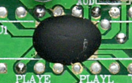
The quest to fabricate more and more devices in a minimum Silicon space has been ON since J. K and R. Noyce invented the first ICs. This quest has enabled scientific community to cross various technological frontiers. Sustained efforts to put more and more transistors on a wafer have led us to nanotechnologies. In the commonly used electronic technology, the semiconductor chips (also known as bare-dice) are individually mounted on a package, and wire-bonded to its I/O pins. This package is then mounted on a Printed Circuit Board (PCB). However, not only does packaging of single chip ICs cost more than the cost of the chips they contain, packaging of a chip take relatively large amount of physical space. Using a conventional single chip package and circuit board interconnect strategy, the package and interconnects took up over 50% of the timing budget as well.

