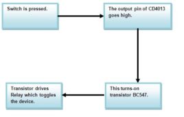
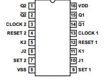
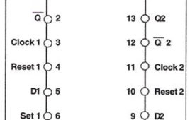
The circuit uses the CMOS dual D type flip flop CD4013 which contains two positive-edge triggered flip flop to toggle a load connected through a relay. Now [[wysiwyg_imageupload::]]with the help of a switch you can on the device once pressing it and off the device again using the same switch. In CD4013 each module is further equipped with a group of pin outs assigned as data, set, reset, clock input and a couple complementary output Q and Q(not) . As we know it has couple of output that change or toggle state as response to trigger applied to input terminals. In this circuit, one is wired in toggle mode while other is not used. Using this circuit we can easily control AC and DC appliances remotely through inexpensive low voltage cable and a standard push to on switch. This circuit can easily support a cable length of 25 meters.
Understanding JK flip flop using CD4027
CD4027 is a common JK Flip flop based IC and if often used as data storing element. It contains two identical or symmetrical JK flip flop. Individual set of flip [[wysiwyg_imageupload::]]flop has provision of pin like set, reset, clock input, J, K and complementary outputs. JK flip flop can be used in applications like registers, counters or as control circuits. CD4027 is a master slave JK flip flop IC which works in toggle mode. Here, this IC can be used to change the state by signal applied to one or more control inputs and will have one or two outputs. In this output not only depends upon the current input. A flip flop is mostly used in computer for its memory circuit. In this circuit, both are opposite of each other for example voltage on Q bar is zero means Q should be having higher voltage.
NOR Gate as SR Flip Flop
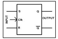
SR Flip flop are the basic element of the sequential circuit. Flip flop is a digital circuit capable of storing single bit of binary data. They can store either of the two [[wysiwyg_imageupload::]]stable state that is binary zero or one. If flip flop is set to one particular state it will store that until power is switched off or until you have changed the state. Means flip flop remember the state it was previously set and memorizes the date provided to it. Here we have designed the SR flip flop with the use of NOR gate. SR flip flop or SR latch is the most essential and widely used flip. It is also known as SET-RESET flip flop. SR flip flop has two inputs S and R. S is used to set the flip flop and R is used to reset the flip flop and two outputs Q and Q(NOT) in this one is complement of another. When flip flop is storing 1 we can said that it is set and while reset it is storing 0.
NAND Gate as SR Flip Flop
SR Flip flops are the basic element of the sequential circuit. Flip flop is a digital circuit capable of storing single bit of binary data. They can store either of the two [[wysiwyg_imageupload::]]stable state that is binary zero or one. If flip flop is set to one particular state it will store that until power is switched off or until you have changed the state. This means that flip flop remembers the state it was previously set and memorizes the data provided to it. Here we have designed the SR flip flop with the use of NAND gate. SR flip flop has two inputs S and R. S is used to set the flip flop and R is used to reset the flip flop and two outputs Q and Q(NOT) in this one is complement of another. When flip flop is storing 1 we can said that it is set and while reset it is storing 0.
Flip Flop based Staircase Switch
In many cases, the stairs have a power switch at the bottom which is often left switched on during night. No one wants to go down to switch it off and hence, [[wysiwyg_imageupload::]]unnecessary on, it leads to wastage of electricity.To solve this problem we have described a simple circuit which contains two micro switches; one at the top and other located at the bottom of the staircase that can be pushed and released easily during climb-up from the bottom of the staircase or climb-down from the top of staircase. In short you can use any switch to on and off the light.This simple circuit is built around a CD4013 IC which has two independent D type flip flops which exist in complimentary states and can store information. Each module is further equipped with a group of pin outs assigned as data, set, reset, clock input and a couple complementary output Q and Not Q.


