
by Ken Ghadia, Sales Engineer, TechnoTronix PCB fabrication is transforming circuit board design into a physical PCB based on design specifications. It is usually an outsourced activity done by a Contract Manufacturer (CM) who strictly follows the specifications provided by the designer. Certain critical factors like choice of the PCB substrate, layout strategy, surface coating requirements…
10 straightforward ways to reduce PCB assembly costs without compromising PCB quality

by Ken Ghadia, Sales Engineer, TechnoTronix It is difficult to build a quality product at the lowest cost. The quality of a PCB depends on the competence of its design for assembly, testing, repair, reliability, manufacturing, and yield. Several factors impact the cost of a PCB assembly. However, the designers can consider certain factors that may…
From designing to operating an RF PCB: The complete guide
by Ken Ghadia, Sales Engineer, TechnoTronix Radio Frequency (RF) PCBs are very high-speed circuits operating at frequencies in the range of 100MHz and above, typically from 500MHz to 2 GHz. RF PCBs are the backbone of wireless networks, high-tech gadgets like smartphones, smart TVs, etc. Also, RF PCBs are used in automotive, medical equipment, military,…
Top ten tips for nailing your PCB silkscreen design
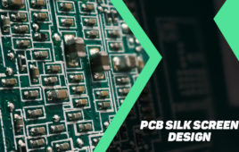
By Suresh Patel, Sales Engineer, Mer-Mar Electronics Silkscreen represents the outer layers of a PCB that include text-based readable information like component reference designator, test points, company logos, PCB part number and version number, etc. This is necessary for circuit board assembly, rework and debug support. The silkscreen ink is different from the regular printing…
PCB Layout Design with Proteus
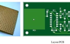
Generally we are listening the wards PCB’s, PCB layout, PCB designing, ect. But what is PCB? Why we are using this PCB? We want to know about all these things as a electronic engineer. PCB means Printed Circuit Board. This is a circuit board with printed copper layout connections. These PCB’s are two types. One is dotted PCB and another one is layout PCB. What is the main difference between the dotted PCB and layout PCB? In dotted PCB board only dots are available. According to our requirement we can place or insert the components in those holes and attach the components with wires and soldering lid. In this dotted PCB we can make the circuit as out wish but it is very hard to design. There are so many difficulties are there. Those are connecting the proper pins, avoiding shot connections and etc. Coming to the layout PCB this is simple to design.