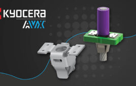
KYOCERA AVX, a global manufacturer of advanced electronic components, has released the new 9296-11X Series STRIPT vertical poke-home through-board contacts for 12–18AWG wire. The new 9296-11X Series vertical through-board contacts further expand the company’s portfolio of user-friendly poke-home contacts and connectors. This addition brings the portfolio total to 10 series, two of which — this series and 9296-000 Series contacts —…
Infineon using recyclable PCBs to minimize electronic waste
With the growing amount of electronic waste generated by consumers, industry, and other sectors, it’s critical to address this specific environmental issue. Reducing the carbon footprint and promoting sustainability are, therefore, key to achieving climate goals and improving environmental protection. This is why Infineon Technologies is taking another important step toward a greener future with…
Renesas to standardize PCB development designs using Altium 365

Renesas Electronics Corporation, a supplier of advanced semiconductor solutions, has announced that it has standardized the development of all printed circuit board (PCB) designs on the Altium 365 cloud-based platform from Altium, LLC, a global software company based in San Diego, California. Renesas currently employs multiple PCB design tools across the company, in part because…
Microchip introduces inductive position sensors for EV motor-control applications

Developers of motor-control systems are rapidly replacing Hall Effect position sensors and older magnetic resolver solutions with inductive alternatives that eliminate expensive magnets and other heavy transformer-based structures so they can be integrated onto simple, compact printed-circuit boards (PCBs). Extending the world’s broadest line of inductive position sensors into the EV motor-control market, Microchip Technology announces…
New shielding options available for Harwin’s Gecko Hi-Rel connectors

Harwin has introduced horizontal backshells for its Gecko-Screw-Lok (Gecko-SL) series of lightweight, high-reliability (Hi-Rel) connectors. These backshells ensure a fully EMI/RFI shielded connection for horizontal 1.25mm pitch board-to-cable connections. Previously, Gecko EMI/RFI shielding was only available on vertical board-to-cable orientations. This new development will be of real value to applications requiring EMI/RFI protection, but where there’s…
Nexperia’s new Zener diodes extend battery-time and save PCB space
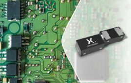
Nexperia, an expert in essential semiconductors, has announced a comprehensive range of low-current voltage regulator diodes. The 50 µA Zener diode range is available in three different surface-mountable (SMD) package options, in an ultra-small discretes flat no-leads (DFN) package and AEC-Q101 qualified parts — providing the ultimate in customer choice and flexibility. Specified at a…
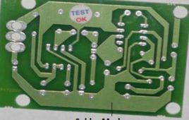
A comprehensive guide to PCB prototype testing
By Arshon Technology For PCB prototype applications, one prerequisite is a must: reliable testing. These early products are built with the sole purpose of testing design ideas to ensure they work for approved use and sale. Be that as it may, PCBs can be unpredictable as there are many parts and patch associations. When electronic…
Diodes offers new 8-channel ReDriver with internal coupling capacitors
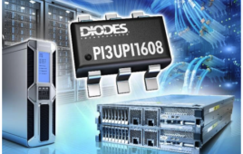
Diodes Incorporated is offering a new addition to its extensive range of linear ReDriver ICs. The PI3UPI1608 helps to significantly extend PCB trace lengths while minimizing power consumption and associated bill-of-materials costs. Supporting speeds of up to 20Gbps, this UPI 2.0 and PCIe 4.0-compliant device has eight differential channels. Its built-in coupling capacitors allow significant…
How to make a PCB Layout
You might have seen that how to make a PCB, but before making PCB you must have knowledge about how to make layout for making PCB. There is quite a bit of software by which youe can make layouts such as KiCad, OrCAD, eagle, spice etc. Here we will discuss about KiCad and we are…
15 PCB Assembly Tips for Electronic Engineers while Dealing with Electronic Projects

Often while working with PCBs, the electronics engineers (particularly students and beginners) face a problem in dealing with the complexity of the circuit boards due to a lack of experience. Breadboards are easy to work with because there is an option to plug in and plug out the components even if you make a mistake in the connection. However, when you switch to PCBs a lot has to be kept in mind whether it’s the soldering, de-soldering, or other related tasks. Although constant practice is crucial to achieving the expertise level, there are a handful number of tips that can level up your chance of success.
Terms used in PCB design
Many of us design PCB with the information available on internet but sometimes it becomes difficult to understand the terms used in designing. In this article I have tried to explain the common terms which are used while designing PCB. PCB stands for printed circuit board. Different types of PCB materials are available in markets. Most commonly used are FR-1, FR-2, CEM-3, CEM-1 (FR=Flame Retardant and CEM= Composite Epoxy Material).Everything which you draw is on layer. Each layer has different physical properties. For example top layer is used to draw the component layout, bottom layer or inner layer are used for making connection between components and many more are also present.
DIY – Battery Powered USB Travel Charger
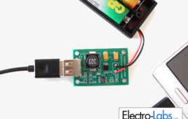
Battery powered devices are all around us in daily life and we always face with low charge problems which lets us down in the middle of the day. Especially phones, music and video players, e-book readers etc. Sometimes we can’t find a mains source to plug an AC adapter or an USB port of a computer. In those cases, the battery powered USB travel charger comes to aid. It can be powered by two or three AA or AAA size batteries which you can find easily or carry with you while you are mobile. This article provides all the steps of the design and the manufacturing process of DIY Battery Powered USB Travel Charger project. We will draw the circuit, and PCB by using SoloPCB tools which are free and powerful to cover all our needs. When we finish the board, we will get the PCBs manufactured by Mass Design which has an ordering system integrated to SoloPCB. After receiving the bare boards, we will solder the components, power the circuit up and finally share the test & performance results.
PCB Layout Design with Proteus
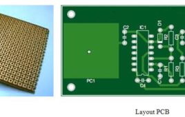
Generally we are listening the wards PCB’s, PCB layout, PCB designing, ect. But what is PCB? Why we are using this PCB? We want to know about all these things as a electronic engineer. PCB means Printed Circuit Board. This is a circuit board with printed copper layout connections. These PCB’s are two types. One is dotted PCB and another one is layout PCB. What is the main difference between the dotted PCB and layout PCB? In dotted PCB board only dots are available. According to our requirement we can place or insert the components in those holes and attach the components with wires and soldering lid. In this dotted PCB we can make the circuit as out wish but it is very hard to design. There are so many difficulties are there. Those are connecting the proper pins, avoiding shot connections and etc. Coming to the layout PCB this is simple to design.
How to make a PCB at home

Often people face problem while making a circuit on a bread board. It is a common problem that the circuit may work some time and may not work other time. Most of the time it is the connections on the bread board which creates this problem. Either are connections are not proper or loose…
Printed Circuit Boards (PCBs) : An Overview
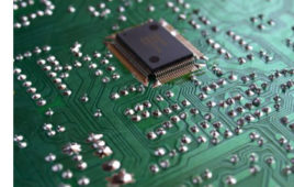
The success of any creation is often dependent on the foundations it is built upon, be it the strength of a character, depth of a building’s foundations or the extent of a tree’s roots. Much in the same way, the success of any electronic device depends on what it is built on. The motherboard of any electronics device serves as a playground and a host to every form of electrical signal that performs some function for the equipment. A Printed Circuit Board doesn’t just connect electrical components using etched copper pathways, but also provides mechanical strength to it. Printed Circuit Boards are found in almost all of the commercial products as a packaging medium as building blocks.
Difference between through hole and Surface mount components
We have certainly come a long way in the field of technology. In the early days people were hardly concerned about the design part of the device. Neither size nor appearance was important. Nowadays, both the features are equally important. These days size of every electronic product is decreasing but the features in these products are increasing. Computer, to laptop, to mobiles in small pocket sizes. One of the reasons for the change is use of Surface mount devices (SMD). Now question arrives what is SMD?As technology grows the demand for less weight and smaller size component increases. This leads to new improved technology known as surface mount technology (SMT). Surface mount components are similar to plated through hole as far as there electrical function is concerned but the key difference is in their size.
PCB Designing using Diptrace Software: Step by Step Tutorial
The efficient laying out of traces on a PCB is a complex skill, and requires much patience. This task has been made vastly easier with the advent of readily available PCB layout software, but it is still challenging.Usually an electronics or electrical engineer designs the circuit, and a layout specialist designs the PCB. There are numerous techniques and standards used to design a PCB that is easy to manufacture and yet small and inexpensive.There are various types of software which are used for PCB designing, In PCB designing first think what is required, a Schematic diagram of the circuit then we have to make a layout by using software and this layout gets printed on the PCB after that Etching, drilling, component placement and soldering are done.