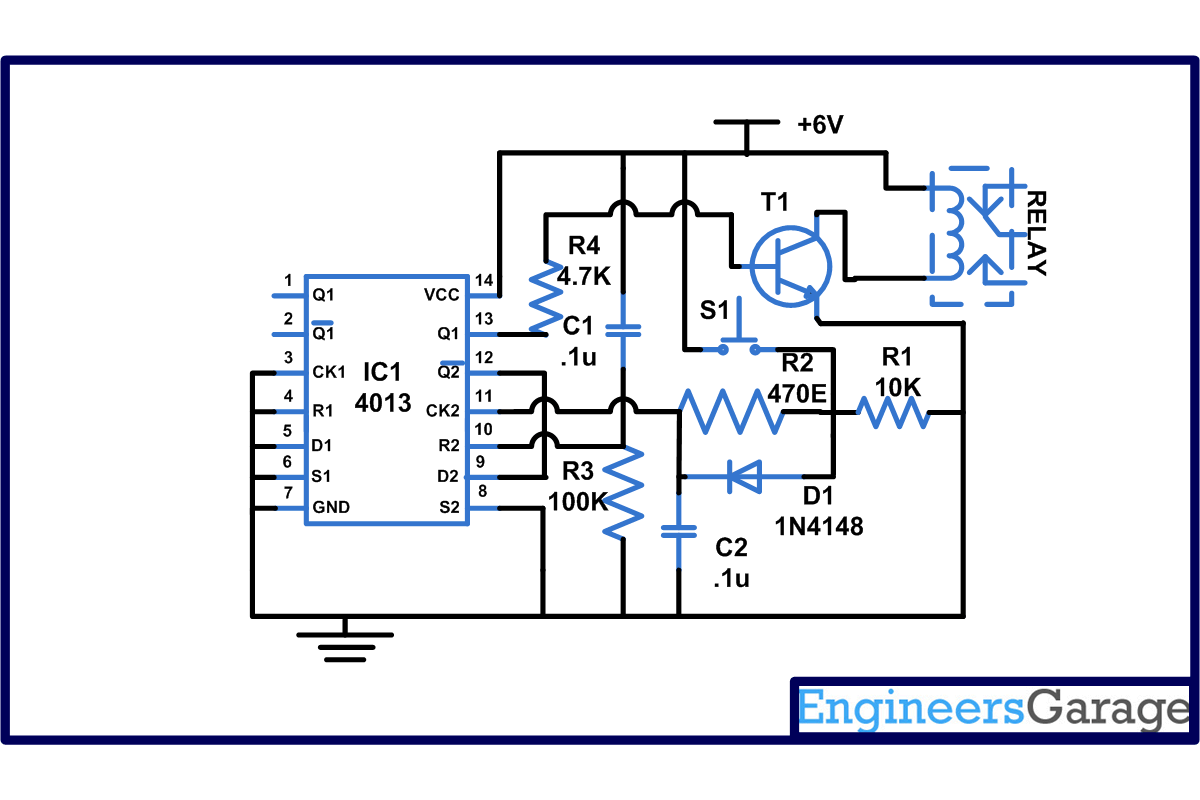
This toggle flip flop circuit uses the CMOS dual D type flip flop CD4013 which contains two positive-edge triggered flip flop to toggle a load connected through a relay. Now with the help of a switch you can on the device once pressing it and off the device again using the same switch.
[[wysiwyg_imageupload:7497:]]
Fig. 1: Pin Out Diagram Of CD4013 IC
In CD4013 each module is further equipped with a group of pin outs assigned as data, set, reset, clock input and a couple complementary output Q and Q(not)
Working of toogle flip flop circuit is very simple: when you press the push to on switch S1, the output pin 13 to change its state from low (device is OFF) to high(device is ON) or vice versa . The output is connected to NPN transistor (BC547) which is used to drive electromagnetic relay as a result device connected to it toggle its state. A clock pulse has been provided at pin 11.

Fig. 2: Block Diagram Of Toogle Flip Flop Circuit
We have connected a capacitor and resistor at pin 10 for safety. These components are assigned to a logic level and generally they are grounded with a high value resistor. Once this is done, the input can be made to alternately respond to positive peak pulses to toggle the logic stage of the Q and {C}{C}{C}{C}{C}{C}{C}{C}{C}{C}{C} output alternately. This means that the combination of C1 and R3 are used to provide power ‘ON’ reset. Resistor R1 and R2, diode D1 and capacitor C2 are used to eliminate the effect of switch bouncing.
Circuit Diagrams
Project Components
Filed Under: Circuit Design

Questions related to this article?
👉Ask and discuss on EDAboard.com and Electro-Tech-Online.com forums.
Tell Us What You Think!!
You must be logged in to post a comment.