Abstract- For low-voltage dc energy sources, a power conditioning system (PCS) is needed to convert the energy sources to a higher-voltage dc before making it to ac for grid tie applications. Fuel cells and Solar photovoltaic (PV) are perhaps the most well-known and prospective energy sources with low voltage dc output. A thermoelectric generator, a battery, and an ultra-capacitor are also examples of such low-voltage dc energy sources. Recently, numerous circuit topologies for the power conversion from low-voltage dc to high-voltage ac for grid-tie applications were proposed to deal with specific issues such as high efficiency, low cost, and safety. The aim of this project is to introduce and discuss the main features of these relatively new circuit topologies that deal with these practical design issues. The whole system is constructed and simulated in MATLAB environment. The power qualities under different conditions are given and compared. An experimental prototype of High efficiency power conditioning system was built and Experimental results are shown to verify the effectiveness of the proposed power conditioning topology.
Index Terms- Dc-to-Dc converter, Pulse Width Modulation (PWM) circuit, H-bridge inverter, Auxiliary devices.
1. INTRODUCTION
The available solar energy resources are 3.8 YJ/yr (120,000 TW). Less than 0.02% of available resources are sufficient to entirely replace fossil fuels and nuclear power as an energy source. Assuming that our rate of usage in 2005 remains constant, we will run out of conventional oil in 2045 and coal in 2159. In practice, neither will actually run out as natural constraints will force production to decline as the remaining reserves dwindle. The rate at which demand increases and reserves dwindle has been increasing dramatically because the rate of consumption is not constant. For example, if demand for oil doubled, reserves would not last as long. In addition, the cost of fossil fuels continues to rise while solar power becomes more economically viable.
In 2007 grid-connected photovoltaic electricity was the fastest growing energy source, with installations of all photovoltaic increasing by 83% in 2009 to bring the total installed capacity to 15 GW.
Nearly half of the increase was in Germany, which is now the world’s largest consumer of photovoltaic electricity (followed by Japan). Solar cell production increased by 50% in 2007, to 3,800 megawatts, and has been doubling every two years. The consumption of solar hot water and solar space heating was estimated at 88 GWt (gigawatts of thermal power) in 2004. The heating of water for unglazed swimming pools is excluded. India is densely populated and has high solar insolation, an ideal combination for using solar power in India. India is already a leader in wind power generation (Wind power in India). Suzlon Energy, based in India is one of the pioneering industries in the world generate non-conventional energy, in this case, wind energy. In the solar energy sector, some large projects have been proposed, and a 35,000 km2 area of the Thar Desert has been set aside for solar power projects, sufficient to generate 700 GW to 2,100 GW (gigawatt).
In July 2009, India unveiled a US$19 billion plan, to produce 20 GW of solar power by 2020. Under the plan, the use of solar-powered equipment and applications would be made compulsory in all government buildings including hospitals and hotels. On November 18, 2009, it was reported that India was ready to launch its National Solar Mission under the National Action Plan on Climate Change, with plans to generate 1,000 MW of power by 2013. The increased in demand for renewable energy has significance over the years because of deficiency of greenhouse effect and fossil fuels. Along with various types of renewable energy sources, wind energy and solar energy have become very popular and increased demand consistently by 20%–25% per annum over the past years, which is mainly due to advancement in power electronics techniques. Photovoltaic (PV) sources are used today in many applications as they have the advantages of being maintenance and pollution free.
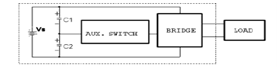
Fig. 1 Five-level PWM inverter
PhotoVoltaic inverter, which is the heart of a PV system, is used to convert dc power obtained from PV modules into ac power to be fed into the grid. The poor quality of current and voltage waveforms of a power system fed by a classical two level inverter has been pointed out in previous works. Therefore the technology of multilevel inverters is very attractive for medium to high voltage range applications and widely used in the power engineering community such as HVDC link, power quality and power conditioning applications, adjustable speed drives. In recent years, multilevel inverters have become more attractive for researchers and manufacturers due to their advantages over conventional pulse width-modulated (PWM) inverters. The advantages of the multilevel inverters compared to conventional two-level inverters are : higher voltage capability, lower total harmonic distortion, lowers switching losses, improved output waveforms, smaller filter size, lower EMI ,lower dv/dt and others . Improving the inverter output waveform in multilevel approach reduces its respective harmonic content and hence reduces the size of the filter used and the level of electromagnetic interference (EMI) generated due to switching operation of the inverter. A multilevel inverter has capability of synthesizing a higher output voltage than the voltage rating of each switching devices, which includes less harmonics at a relatively low switching frequency Among various topologies of multilevel inverter with different control strategies harmonic reduction is limited in certain level but not for all. This project presents a five-level PWM inverter, as the number of output levels increases then the harmonic content can be reduced further. Because of the high conversion ratio DC-DC converter is used in a Power Conditioning system which has quick-response characteristics.
A typical single-phase three-level inverter adopts full-bridge configuration by using approximate sinusoidal modulation technique as the power circuits. The output voltage then has the following three values: zero, positive (+Vdc), and negative (–Vdc) supply dc voltage (assuming that Vdc is the supply voltage). The harmonic components of the output voltage are determined by the carrier frequency and switching functions. Therefore their harmonics reduction is limited to a certain degree[3]. To overcome this limitation, this paper presents a five-level PWM inverter whose output voltage can be represented in the following five levels: zero, +1/2Vdc, Vdc,–1/2Vdc, and –Vdc. As the number of output levels increases, the harmonic content can be reduced. This inverter topology uses two reference signals, instead of one reference signal, to generate PWM signals for the switches. Both the reference signals Vref1 and Vref2 are identical to each other, except for an offset value equivalent to the amplitude of the carrier signal Vcarrier, as shown in Fig. 1. Simulation and experimental results are presented to validate the proposed inverter configuration.
2. SINGLE PHASE THREE LEVEL BRIDGE INVERTER
2.1. Generation of Triggering Signals
The triggering signals used for power switches can be generated by the methods of PWM techniques. In this method the reference wave of sinusoidal with particular amplitude is compared with the triangular carrier wave. The inverter output frequency depends upon the reference sine wave frequency and switching frequency of inverter depends upon the carrier frequency of triangular wave because the high frequency triangular wave is used as a carrier in order to achieve the high values of accuracy as well as stability of the system. Here the PWM triggering signals applied to inverters can be derived from electronic hard ware circuits.[4]
2.2. Sinusoidal pulse width modulation
Instead of maintaining the width of all pulses the same as in the case of multiple pulse modulations, the width of each pulse is varied in proportion to the amplitude of a sine wave evaluated at the center of the same pulse. The distortion factor and harmonics are reduced significantly. Comparing a sinusoidal reference signal with a triangular carrier wave frequency generates the gating signals. This sinusoidal pulse width modulation is commonly used in industrial applications. The frequency of reference signal determines the inverter output frequency and its peak amplitude controls the modulation index and then in turn the RMS output voltage.
2.3. Generation of gating signals
1. Generate a triangular carrier signal with specific amplitude
2. Generate reference signal with specific amplitude
3. Both signals are compared and output produces PWM pulses
4. Output frequency of inverter depends upon the reference wave frequency
5. Switching frequency of inverter depends upon the carrier wave frequency
2.4.Basic principles of operation of PWM inverter
Single-phase inverters are widely used in industrial applications such as induction heating, standby power supplies and uninterruptible supplies. A block diagram representation of a single-phase inverter is given in Fig.2. The inverter consists of four switching devices (represented as ideal switches) connected in the form of a bridge. The control scheme is implemented using. In the uni-polar switching scheme the output voltage changes between positive and zero, or between zero and negative voltage levels. To produce a sinusoidal output voltage waveform of variable frequency and amplitude, a sinusoidal reference signal (Vref) is compared with the triangular waveform (Vtri). The amplitude modulation index (ma), which controls the rms value of the output voltage, is defined as
Ma = Vref/Vtri
The ref V ref and Vtri in equation refer to the peak amplitudes of the signals. Leg A and B of the full-bridge inverter are controlled separately by comparing Vtri with Vref and Vtri with -Vref. The resulting waveforms are used to control the switches as follows:
In leg A
Vref > Vtri: GS1 on and
Vref <Vtri : GS4on
and
In leg B
-Vref > Vtri : GS3 on and
-Vref< Vtri : GS2 on
The PWM signals obtained are shown in Fig 3. Note that GS4 and GS2 will be automatically created as the inversion of GS1 and GS3, respectively [4].
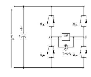 Fig.2. Single phase PWM inverter
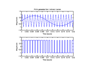
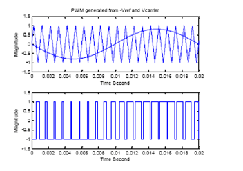
FIG. 3.Generation of PWM signals to Leg A and Leg B
A typical single-phase three-level inverter adopts full-bridge configuration by using approximate sinusoidal modulation technique as the power circuits. The output voltage then has the following three values: zero, positive (+Vdc), and negative (–Vdc) supply dc voltage (assuming that Vdc is the supply voltage). The harmonic components of the output voltage are determined by the carrier frequency and switching functions. Therefore, their harmonic reduction is limited to a certain
degree [3].
3.PROPOSED TOPOLOGY
3.1. DC – DC COVERTER
A Dc-to-Dc converter is an electronic circuit which converts a source of direct current (DC) from one voltage level to another. Switch-mode DC to DC converters convert one DC voltage level to another, by storing the input energy temporarily and then releasing that energy to the output at a different voltage. The storage may be in either magnetic field storage components (inductors, transformers) or electric field storage components (capacitors). Most DC-to-DC converters are designed to move power in only one direction, from the input to the output. Energy is periodically stored into and released from a magnetic field in an inductor or a transformer, typically in the range from 300 kHz to 10 MHz. By adjusting the duty cycle of the charging voltage (that is, the ratio of on/off time), the amount of power transferred can be controlled.[4].
3.2 Step-up(boost)converter
The Boost converter takes a DC input voltage and produces a DC output voltage that is higher in value than the input (but of the same polarity). As the name suggests its output voltage is always greater than the input voltage. A step up converter by switched inductance topology is shown in fig. 4.1. It consists of source voltage Vin and output Vo. The inductors L1 and L2, L1=L2, Diodes D0, D1, D2 and D3, Capacitor C0 and Resistance R0 connected as shown in the topology.
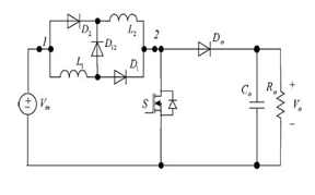
Fig. 4. Step up Converter by Switched Inductor Structure
When the switch S is in ON state (during TON), the inductors L1 and L2 are charged in parallel.
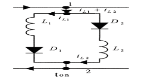
Fig. 5 Switch ON state operation
When the switch is in OFF state (during TOFF), the inductors are discharged in series.
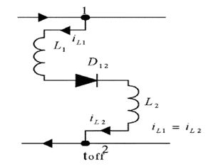
Fig. 6.Switch OFF state operation
The load current is supplied by the two inductors L1 and L2 when the switch is off, and by the output capacitor when the switch is on. The output voltage Vo is given by (for the Boost Converter)
Output Vo = Vin ((1+D)/ D1)
Where D1 = (1-D)
A dc gain times bigger than that of a classical boost converter is obtained. The duality between switching-inductor and switching-capacitor cells was rigorously studied in [2] by using the graph theory.
Thus the step up voltage gain is given by,
Voltage Gain (Vo /Vin ) = ((1 + D)/ D1)
It has been proved that the switched Inductor/ Capacitor type of Boost converter provides high step up voltage gain compared to conventional Boost converter circuit. The main advantages the modified boost type with switched inductor technique are that their structure is very simple, they are transformer less and only one power stage is used .
3.3Pulse width modulation
All of the switching converters use a form of output voltage regulation known as Pulse Width Modulation (PWM). It adjusts the output voltage by changing the ON time (i.e. duty cycle) of the switching element in the converter.

Fig. 5 Generation of PWM wave.
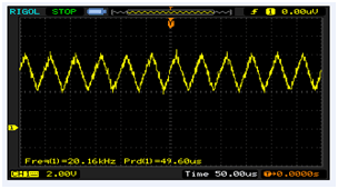
Fig. 6 Simulated Triangular wave.

Fig.7 Simulated PWM wave.
Duty cycle (D) is the fraction of time during which the switch is on. It is the ratio of ON time of the switch to the Total time period (ON time + OFF Time). It values varies between 0 – 1 [5].
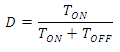
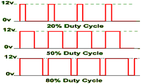
Fig.8 Different duty cycle.
3.4. Selective harmonic elimination PWM
In order to achieve a wide range of modulation indexes with minimized THD for the synthesized waveforms, a generalized selective harmonic modulation method was proposed, which is called virtual stage PWM. An output waveform is shown in Figure 9. The Virtual Stage PWM is a combination of Unipolar Programmed PWM and the fundamental frequency switching scheme. When Unipolar Programmed PWM is employed on a multilevel converter, typically one DC voltage is involved, where the switches connected to the DC voltage are switched “on” and “off” several times per fundamental cycle. The switching pattern decides what the output voltage waveform looks like.
Fig.9.Unipolar switching output waveform
Bipolar Programmed PWM and Unipolar Programmed PWM could be used for modulation indices too low for the applicability of the multilevel fundamental frequency switching method. Virtual Stage PWM can also be used for low modulation indices. Virtual Stage PWM will produce output waveforms with a lower THD most of the time. Therefore, Virtual Stage PWM provides another alternative to Bipolar Programmed PWM and Unipolar Programmed PWM for low modulation index control[5].
3.5 H-bridge inverter
H-bridge stage with an auxiliary bidirectional switch, drastically reducing the power circuit complexity. In the modulator circuit, the Microcontroller can perform all required modulation functions, providing another important reduction in cost and circuit complexity. The new converter topology used in the power stage offers an important improvement in terms of lower component count and reduces layout complexity when compared with five level converters presented in the literature. The new topology achieves almost a 40% reduction in the number of main power switches required and uses no more diodes or capacitors that the second best topology, the asymmetric cascade configuration .The new topology is a single phase configuration that can be used in three phase applications where an open delta primary is acceptable.
The H-Bridge is formed by the four main power devices, switch 1 to switch 4. A capacitor voltage divider, formed by C1 and C2 provides a half supply voltage point.The auxiliary switch, formed by the controlled switch 5 and the four diodes, D1 to D4,connects the center point of the left hand half-bridge to node.
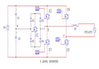
Fig.10 Proposed five Level Inverter Configurations.
3.6. Stage Advantages
To probe the reduction in component numbers achieved by this new configuration, Table I presents the number of components required to implement a five-level inverter using the new topology and three previously defined ones: the two that can be considered as the standard multilevel stages, the diode clamped and the capacitor clamped configurations, and a new and highly improved multilevel stage, the asymmetric cascade configuration Give Table I indicates the comparison between four different five-level inverter topologies. A resistive load and the same output waveform were considered in all the cases. In order to compare the results, the voltage and the current magnitude in the power switches were normalized to the maximum voltage and current in the converter output. This allows comparing different topologies with different DC bus voltages. The results were as follows.
3.7. Main power switches
The new topology achieves a 37.5% reduction in the number of main power switches required, using only 5 controlled power switches instead of the eight required in any of the other three configurations. The auxiliary switch voltages and the current ratings are lower than the ones required by the main controlled switches.
3.8 Auxiliary devices (diodes, capacitor)
The new configuration reduces the number of diodes by 60 %( eight instead of 20) and the number of capacitors by 50 %( two instead of four) when compared with the diode clamped configurations. The new configuration reduces the number of capacitors by 80 %( two instead of 10) when compared with capacitor clamped configuration. The new configuration uses no more diodes or capacitors that the second best topology in the table, the symmetric cascade configuration. Additionally, since the two capacitors are connected in parallel with the main dc power supply, no significant capacitor voltage swing is produced during normal operation, avoiding a problem that can limit operating range in some other multilevel configurations.
Power stage operation
The required five voltage output levels
(Vs, Vs/2, 0,-Vs/2,-Vs)
Maximum positive output (Vs)
Switch1 is ON, connecting the load positive terminal to Vs, and switch 4 is ON, connecting the load negative terminal to ground. All other controlled switches are OFF; the voltage applied to the load terminal is Vs. Fig.9 shows the current paths that are active at this stage.
Half-level positive output (Vs/2)
The auxiliary switch, switch 5 is ON, connecting the load positive terminal to point A, through diodes D5 and D8, and switch 4 is ON, connecting the load negative terminal to ground. All other controlled switches are OFF; the voltage applied to the load terminals is Vs/2.
Zero output
The two main switches switch3 and switch4 are ON, short-circuiting the load. All other controlled switches are OFF; or the main switches switch1 and switch2 are ON, short-circuiting the load. All other controlled switches are OFF; the voltage applied to the load terminal is zero.
Half-level negative output (-Vs/2):
The auxiliary switch, switch 5 is ON, connecting the load positive terminal to point A, through diodes D6 and D7, and switch 2 is ON, connecting the load negative terminal to Vs. All other controlled switches are OFF; the voltage applied to the load terminals is (-Vs/2).
Maximum negative output (-Vs):
Switch2 is ON, connecting the load negative terminal to Vs, and switch3 is ON, connecting the load positive terminal to ground. All other controlled switches are OFF; the voltage applied to load terminals is (-Vs).Fig.9 shows the current paths that are active at this stage. . In this configuration the two capacitors in the capacitive voltage divider are connected directly across the DC bus, and since all switching combinations are activated in an output cycle, the dynamic voltage balance between the two capacitors is automatically restored. The switching combinations that generate the required five output levels (Vs, Vs/2, 0,-Vs/2,-Vs).

Fig.9 waveform of 5-level output.
Table.1
Switching combinations required to generate the five-level output voltage waveform
|
S1
|
S2
|
S3
|
S4
|
S5
|
Vout
|
|
OFF
|
ON
|
OFF
|
OFF
|
ON
|
+VS
|
|
ON
|
OFF
|
OFF
|
OFF
|
ON
|
+VS/2
|
|
OFF
|
OFF
Or
ON
|
OFF
Or
ON
|
ON
Or
OFF
|
ON
Or
OFF
|
0
|
|
ON
|
OFF
|
OFF
|
ON
|
OFF
|
-VS/2
|
|
OFF
|
OFF
|
ON
|
ON
|
OFF
|
-VS
|
Results and Description
3 .10 RESULT AND DISCUSSION
The result of single phase multilevel pv inverter is shown below. Harmonic distortion measurement has been carried out to compare the harmonic distortion of the three-level PWM inverter with that of the five-level PWM inverter for PV application.
CASE I : 3 LEVEL INVERTER 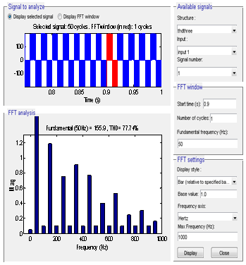
Fig.10 magnitude Vs frequency with various harmonic distortion
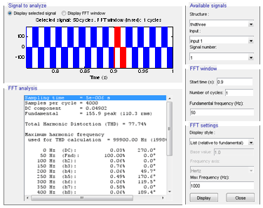
Fig.11 Analysis of harmonic distortion with various frequencies.
With help of above figures, it is shown that THD is 77.74% with various frequencies.
CASE II: 5 LEVEL INVERTER 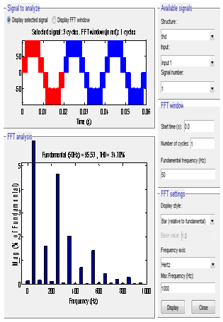
Fig. 12 Magnitude Vs Frequency with various harmonic distortion.
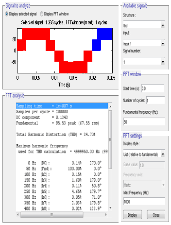
Fig.13 Analysis of harmonic distortion with various frequencies.
With help of above figures, it is shown that THD is 34.70% with various frequencies.
On Comparing both different levels,we can conclude that THD is less in 5-level topology which is easier to implement in grid.
4. CONCLUSION
This paper presented a single-phase multilevel inverter for PV application. It utilizes reference signals and a carrier signal to generate PWM switching signals. The circuit topology, modulation law, and operational principle of the proposed inverter were analyzed in detail. Experimental results indicate that the THD of the five-level inverter is much lesser than that of the conventional three-level inverter. Furthermore, both the grid voltage and the grid current are in phase at near-unity power factor.
Project Source Code
Filed Under: Electronic Projects

Questions related to this article?
👉Ask and discuss on Electro-Tech-Online.com and EDAboard.com forums.
Tell Us What You Think!!
You must be logged in to post a comment.