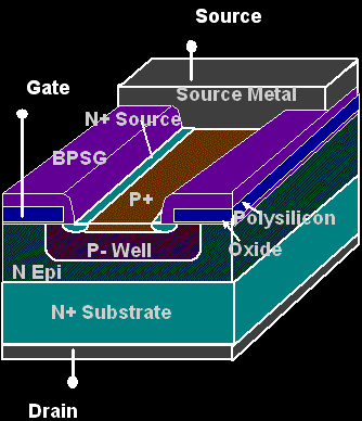
Trench MOSFET technology is the newly introduced MOSFET technology in which the gate electrode of the MOSFET is buried in trench etched in Silicon to get a vertical structure to enhance the channel density. The MOSFET using the trench gate is called TrenchMOS or UMOS (since the trench is U shaped).The main feature of TrenchMOS is that it lacks the JFET effect.

Trench technology is widely used in devices of Laptops and Note book computers, UPS etc because of the great power density and very little power dissipation. Trench technology requires only less than ten mask steps in silicon fabrication. This helps to increase the physical size of the device to accommodate requirements such as high voltage and current.

The Trench MOSFET has a field plate that extends into the drift region which is electrically coupled with the source. This arrangement helps to deplete the drift region when the MOSFET turns off. Unlike other planar Power MOSFETS, trench MOSFET is used in low voltage applications. The advantages of trench technology includes, fast switching, forward voltage stability and good performance in high frequency ranges. The MOSFET has a heat sink attached during fabrication for easy heat dissipation in the device.
One most commonly used Trench MOSFET is PSMN 004-25 B. Most of the UPS systems use this MOSFET because of its reliability. It is also used in SMPS and DC-DC converters. The features of this MOSFET are fast switching, very low on-state resistance and low thermal resistance. It can handle maximum 25 volts and very high current. Power handling capacity is 25 Watts.
Pin assignment ( Front view) of PSMN 004-25B
 Pin 1 – Gate
Pin2 – Drain1
Pin3 – Source
Tab – Drain
Filed Under: Electronic Projects

Questions related to this article?
👉Ask and discuss on Electro-Tech-Online.com and EDAboard.com forums.
Tell Us What You Think!!
You must be logged in to post a comment.