This is the Article to introduce the UART (Universal Asynchronous receiver/Transmitter) programming of ARM Cortex-M3 LPC1768 Microcontroller. Here we are going to receive serial data from PC and echo back the same data while displaying the same on the LCD. Setting up the Environment for the development ofARM cortex M3 is well discussed in this article.
The LPC 1768 is ARM Cortex- M3 based Microcontrollers for embedded application features in low power consumption and a high level of integration. The ARM Cortex M3 is designed in a such way to enhance debug features and a higher level of system integration. It clocks at a CPU frequency of 100 MHz, and incorporates a 3-stage pipeline and uses a Harvard architecture with separate local instruction and data buses for third bus peripherals. The ARM Cortex- M3 CPU have an internal pre-fetch unit to support speculative branching. The peripheral components include 512KB of flash memory, 64kb of data memory, Ethernet MAC, USB OTG, 4 UART’s, 8-channel general purpose DMA controller, 2 SSP Controllers, 10-bit DAC, Quadrature encoder interface, SPI interface, 3 I2C bus interface, 2 input plus 2 outputs I2S bus interface, 4 general purpose timers, ultra-low power Real-Time Clock (RTC) with separate battery supply, and up to 70 general purpose I/O pins, 6-output general purpose PWM. The LPC1768/66/65/64 are pin-compatible with the 100-pin LPC236x ARM7-based Microcontroller series.

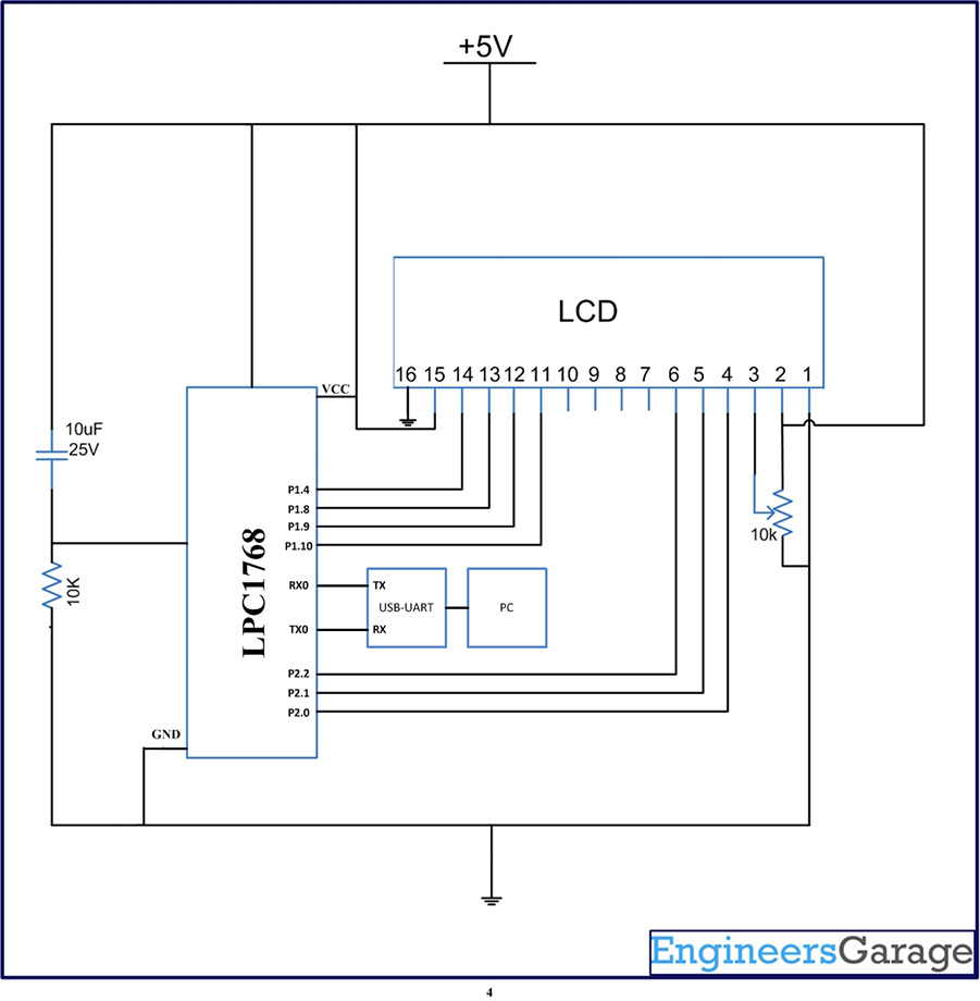
Fig. 1: UART Programming In LPC1768 Prototype
The ARM Cortex M3(NXP LPC1768) contains 4 UARTs numbering fro 0 to 3, similarly the name of the pins also RXD0,TXD0 to RXD3,TXD3. The UART module of LPC1768 can be of 5,6,7,and 8 bits wide with parity generation and checking. It includes one or two stop bits. It has built-in baud rate generator, including a fractional rate divider for great versatility. It also support for software flow control.
POWERING THE UART:
PCON register bits description:
|
Bit |
Symbol |
Description |
Reset value |
|
0 |
– |
Reserved. |
NA |
|
1 |
PCTIM0 |
Timer/Counter 0 power/clock control bit. |
1 |
|
2 |
PCTIM1 |
Timer/Counter 1 power/clock control bit. |
1 |
|
3 |
PCUART0 |
UART0 power/clock control bit. |
1 |
|
4 |
PCUART1 |
UART1 power/clock control bit. |
1 |
|
5 |
– |
Reserved. |
NA |
|
6 |
PCPWM1 |
PWM1 power/clock control bit. |
1 |
|
7 |
PCI2C0 |
The I2C0 interface power/clock control bit. |
1 |
|
8 |
PCSPI |
The SPI interface power/clock control bit. |
1 |
|
9 |
PCRTC |
The RTC power/clock control bit. |
1 |
|
10 |
PCSSP1 |
The SSP 1 interface power/clock control bit. |
1 |
|
11 |
– |
Reserved. |
NA |
|
12 |
PCADC |
A/D converter (ADC) power/clock control bit. |
0 |
|
13 |
PCCAN1 |
CAN Controller 1 power/clock control bit. |
0 |
|
14 |
PCCAN2 |
CAN Controller 2 power/clock control bit. |
0 |
|
15 |
PCGPIO |
Power/clock control bit for IOCON, GPIO, and GPIO interrupts. |
1 |
|
16 |
PCRIT |
Repetitive Interrupt Timer power/clock control bit. |
0 |
|
17 |
PCMCPWM |
Motor Control PWM |
0 |
|
18 |
PCQEI |
Quadrature Encoder Interface power/clock control bit. |
0 |
|
19 |
PCI2C1 |
The I2C1 interface power/clock control bit. |
1 |
|
20 |
– |
Reserved. |
NA |
|
21 |
PCSSP0 |
The SSP0 interface power/clock control bit. |
1 |
|
22 |
PCTIM2 |
Timer 2 power/clock control bit. |
0 |
|
23 |
PCTIM3 |
Timer 3 power/clock control bit. |
0 |
|
24 |
PCUART2 |
UART 2 power/clock control bit. |
0 |
|
25 |
PCUART3 |
UART 3 power/clock control bit. |
0 |
|
26 |
PCI2C2 |
I2C interface 2 power/clock control bit. |
1 |
|
27 |
PCI2S |
I2S interface power/clock control bit. |
0 |
|
28 |
– |
Reserved. |
NA |
|
29 |
PCGPDMA |
GPDMA function power/clock control bit. |
0 |
|
30 |
PCENET |
Ethernet block power/clock control bit. |
0 |
|
31 |
PCUSB |
USB interface power/clock control bit. |
0 |
Fig. 2: Bits Description Of PCON Register In LPC1768
Following reset the PCUART0 and PCUART1 (Power Clock Control Bit to UART) bits are set and these two are enabled. But PCUART2 and PCUART3 (Power Clock Control Bit to UART) bits are cleared and these two are disabled. The first step while using these UARTs is to set PCUARTx bits. In this article we are going to use UART0.
SELECTING THE CLOCK FOR UART:
By assuming that the main clock for the LPC1768 has been programmed. Each LPC1768 peripheral including the UART has a clock derived from the main clock as illustrated.
Peripheral Clock Divider
As shown in the below block the frequency of the peripheral clock is determined by two bits in the PCLKSEL registers. UART0 is included in PCLKSEL0. With the NXP LPC1768 the peripheral clocks are always active. Following RESET, PCLKSEL registers are cleared setting the peripheral clock frequency to CCLK/4 to all the peripherals. The user will have a choice of frequency which can be determined by two bits for each peripherals among the peripheral clock selection registers PCLKSEL0 and PCLKSEL1. By default at reset all values are 00 ie CCLK/4.
|
00 |
PCLK_peripheral = CCLK/4 |
|
01 |
PCLK_peripheral = CCLK |
|
10 |
PCLK_peripheral = CCLK/2 |
|
11 |
PCLK_peripheral = CCLK/8, except for CAN1, CAN2, |
Fig. 3: Bit Value Of PCLK_Peripheral For Clock Frequency
|
Bit |
Symbol |
Description |
|
1:0 |
PCLK_WDT |
Peripheral clock selection for WDT. |
|
3:2 |
PCLK_TIMER0 |
Peripheral clock selection for TIMER0. |
|
5:4 |
PCLK_TIMER1 |
Peripheral clock selection for TIMER1. |
|
7:6 |
PCLK_UART0 |
Peripheral clock selection for UART0. |
|
9:8 |
PCLK_UART1 |
Peripheral clock selection for UART1. |
|
11:10 |
– |
Reserved. |
|
13:12 |
PCLK_PWM1 |
Peripheral clock selection for PWM1. |
|
15:14 |
PCLK_I2C0 |
Peripheral clock selection for I2C0. |
|
17:16 |
PCLK_SPI |
Peripheral clock selection for SPI. |
|
19:18 |
– |
Reserved. |
|
21:20 |
PCLK_SSP1 |
Peripheral clock selection for SSP1. |
|
23:22 |
PCLK_DAC |
Peripheral clock selection for DAC. |
|
25:24 |
PCLK_ADC |
Peripheral clock selection for ADC. |
|
27:26 |
PCLK_CAN1 |
Peripheral clock selection for CAN1.[1] |
|
29:28 |
PCLK_CAN2 |
Peripheral clock selection for CAN2.[1] |
|
31:30 |
PCLK_ACF |
Peripheral clock selection for CAN acceptance filtering.[1] |
Fig. 4: Bit Value And Description Of PCLK_Peripheral Register In LPC1768
Code snipet:
Function to set the peripheral clock for timer 0 to divide by 8 of the system clock frequency.
pclkdiv = (LPC_SC->PCLKSEL0 >> 6) & 0x03;
switch ( pclkdiv )
{
case 0x00:
default:
pclk = SystemFrequency/4;
break;
case 0x01:
pclk = SystemFrequency;
break;
case 0x02:
pclk = SystemFrequency/2;
break;
case 0x03:
pclk = SystemFrequency/8;
break;
}
BAUDRATE CALCULATION:
LPC1768 generates the baud rate depending on the values of Divisor latch registers DLL and DLM.
|
DLL and DLM : Divisor latch registers |
|||
|
Speed (bps) |
Divisor |
DLL |
DLM |
|
50 |
2,304 |
0x00 |
0x09 |
|
300 |
384 |
0x80 |
0x01 |
|
1,200 |
96 |
0x60 |
0x00 |
|
2,400 |
48 |
0x30 |
0x00 |
|
4,800 |
24 |
0x18 |
0x00 |
|
9,600 |
12 |
0x0C |
0x00 |
|
19,200 |
6 |
0x06 |
0x00 |
|
38,400 |
3 |
0x03 |
0x00 |
|
57,600 |
2 |
0x02 |
0x00 |
|
115,200 |
1 |
0x01 |
0x00 |
Fig. 5: Baud Rate In LPC1768 With Divisor Latch Registers DLL And DLM
Baudrate = PCLK/ (16 * ( 256 * DLM + DLL) * (1+ DivAddVal/MulVal))
Getting the PCLK value.
PCLKSELx registers contain the PCLK info for all the clock dependent peripherals in which Bit6,Bit7 contains the Uart Clock(ie.UART_PCLK) information.
The UART_PCLK and the actual Peripheral Clock(PCLK) is calculated as discussed above.
Using the above parameters , DLL/DLM is calculated as below.
(256 * DLL + DLM) = PCLK / (16* Baudrate).
Code snippet:
Fdiv = ( pclk / 16 ) / baudrate ; /*baud rate */
LPC_UART0->DLM = Fdiv / 256; LPC_UART0->DLL = Fdiv % 256;
SELECTING THE UART FUNCTION TO GPIO:
All the pins of LPC1768 has alternate functions to the default digital input-output functions we have to first select the pin for the appropriate function. The second alternate function for P0.2 and P0.3 are TXD0 and RXD0. As we discussed in the previous articles the GPIO function is selected with the help of PINSEL register of the Pin control block. Port 1 is controlled by PINSEL0,1 and Port 1 is controlled by PINSEL2,3. RESET makes all the bits of PINSEL to be cleared results in attachment of GPIO function to the pins.
Each pin is controlled by 2 consecutive bits of PINSEL register. PINSEL0[1:0] bits controls the Pin P0.0, PINSEL0[3:2] bits controls the Pin P0.1. PINSEL0[31:30] bits controls the Pin P0.15, etc.- PSEL3[31:30] bits will control the pins Pin P1.31. The UART0 pins are attached to pins P0.2 and P0.3. The following code will select alternate function 1.
Below table shows the multiplexed UARTs pins.
|
Port Pin |
Pin Functions |
Associated PINSEL Register |
|
P0.2 |
0-GPIO, 1-TXD0, 2-AD0[7], 3- |
4,5 bits of PINSEL0 |
|
P0.3 |
0-GPIO, 1-RXD0, 2-AD0[6], 3- |
6,7 bits of PINSEL0 |
|
P0.10 |
0-GPIO, 1- TXD2, 2- SDA2, 3- MAT3[0] |
20,21bits of PINSEL1 |
|
P0.11 |
0-GPIO, 1- RXD2, 2- SCL2, 3- MAT3[1] |
22,23 bits of PINSEL1 |
|
P0.15 |
0-GPIO, 1- TXD1, 2- SCK0 , 3- SCK |
30,31 bits of PINSEL1 |
|
P0.16 |
0-GPIO, 1- RXD1, 2- SSEL0, 3- SSEL |
1,2 bits of PINSEL2 |
|
P0.25 |
0-GPIO, 1-AD0[2], 2-I2SRX_SDA, 3-TXD3 |
18,19 bits of PINSEL1 |
|
P0.26 |
0-GPIO, 1-AD0[3], 2-AOUT, 3-RXD3 |
20,21 bits of PINSEL1 |
Fig. 6: UARTs multiplexed pins With PINSEL Register In LPC1768
Code snipet:
LPC_PINCON->PINSEL0 &= ~0x000000F0;
LPC_PINCON->PINSEL0 |= 0x00000050; /* RxD0 is P0.3 and TxD0 is P0.2 */
UART REGISTERS AND ITS CONFIGURATION:
Configuration of the individual registers for UART communication is discussed below.
FCR ( FIFO Control Register ):
LPC1768 has inbuilt 16bytes of buffer register called FIFO for the transmission and reception. It implies that it can store 16bytes of data received without overwriting. If the FIFO register is full OVERRUN error will be set.
|
Bit |
Symbol |
Description |
Reset Value |
|
0 |
FIFO ENABLE |
This bit is used to enable/disable the FIFO for the data received/transmitted. 0–FIFO is Disabled. 1–FIFO is Enabled for both Rx and Tx. |
0 |
|
1 |
RX FIFO RESET |
This is used to clear the 16-byte Rx FIFO. 0–No impact. 1–CLears the 16-byte Rx FIFO and the resets the FIFO pointer. |
0 |
|
2 |
TX FIFO RESET |
This is used to clear the 16-byte Tx FIFO. 0–No impact. 1–Clears the 16-byte Tx FIFO and the resets the FIFO pointer. |
0 |
|
3 |
DMA MODE |
This is used for Enabling/Disabling DMA mode. 0–Disables the DMA. 1–Enables DMA only when the FIFO(bit-0) bit is SET. |
0 |
|
5:4 |
– |
Reserved, user software should not write ones to reserved bits. The value read from a reserved bit is not defined. |
NA |
|
7:6 |
RX TRIGGER |
This bit is used to select the number of bytes of the receiver data to be written so as to enable the interrupt/DMA. 00– Trigger level 0 (1 character or 0x01) 01– Trigger level 1 (4 characters or 0x04) 10– Trigger level 2 (8 characters or 0x08) 11– Trigger level 3 (14 characters or 0x0E) |
00 |
|
31:8 |
– |
Reserved, user software should not write ones to reserved bits. The value read from a reserved bit is not defined. |
NA |
LCR ( Line Control Register ):
This register is used for defining the UART frame format ie. Number of Data bits, STOP bits etc.
|
Bit |
Symbol |
Description |
Reset Value |
|
1:0 |
Word Length Select |
These two bits are used to select the character length 00– 5-bit character length 01– 6-bit character length 10– 7-bit character length 11– 8-bit character length |
00 |
|
2 |
Stop Bit Select |
This bit is used to select the number(1/2) of stop bits 0– 1 Stop bit 1– 2 Stop Bits |
0 |
|
3 |
Parity Enable |
This bit is used to Enable or Disable the Parity generation and checking. |
0 |
|
5:4 |
Parity Select |
These two bits will be used to select the type of parity. 00– Odd parity. Number of 1s in the transmitted character and the attached parity bit will be odd. 01– Even Parity. Number of 1s in the transmitted character and the attached parity bit will be even. 10– Forced “1” stick parity. 11– Forced “0” stick parity |
00 |
|
6 |
Break Control |
0– Disable break transmission. 1– Enable break transmission. Output pin UARTn TXD is forced to logic 0 |
0 |
|
7 |
DLAB |
Divisor Latch Access Bit This bit is used to enable the access to divisor latch. 0– Disable access to divisor latch 0– Enable access to divisor latch |
|
|
31:8 |
Reserved |
Reserved, user software should not write ones to reserved bits. The value read from a reserved bit is not defined. |
NA |
LSR (Line Status Register):
The is a read-only register that provides status information of the UART TX and RX blocks.
|
Bit |
Symbol |
Description |
Reset Value |
|
0 |
RDR |
Receive Data Ready |
0 |
|
1 |
OE |
Overrun Error |
0 |
|
2 |
PE |
Parity Error |
0 |
|
3 |
FE |
Framing Error |
0 |
|
4 |
BI |
Break Interrupt |
0 |
|
5 |
THRE |
Transmitter Holding Register Empty |
0 |
|
6 |
TEMT |
Transmitter Empty |
0 |
|
7 |
RXFE |
Error in Rx FIFO |
0 |
|
31:8 |
Reserved |
Reserved, user software should not write ones to reserved bits. The value read from a reserved bit is not defined. |
NA |
TER (Transmitter Enable register)
This register is used to Enable/Disable the transmission
|
Bit |
Symbol |
Description |
Reset Value |
|
6:0 |
Reserved |
Reserved, user software should not write ones to reserved bits. The value read from a reserved bit is not defined. |
NA |
|
7 |
TXEN |
Trsnamitter Enable Note: By default this bit will be set after Reset. |
0 |
|
31:8 |
Reserved |
Reserved, user software should not write ones to reserved bits. The value read from a reserved bit is not defined. |
NA |
Create a project using Keil uvision4 for LPC1768 Microcontroller:
In this section, we will start creating a project in Keil MDK we have already installed Keil µVision and Co-MDK Plug-in + CoLinkEx Drivers required for the CoLinkEx programming adapter. You can start by downloading the project files and kick start your practical experiment which includes all libraries and the source codes for the UART in LPC1768.
Code Description:
Separate functions are used for UART initialization, UART interrupt handling, and APIs for UART access.
The function used for the UART initialization is
UARTInit(0, 57600); /* baud rate setting */
Here 0 defines the UART0 and 57600 is the baud rate.
To send a data by UART this function is used.
UARTSend( 0, (uint8_t *)UART0Buffer, UART0Count );
Here 0 tells it is UART0 and the data to be send is the same which is received.
For more details on interfacing the LCD in 4 bit mode with LPC1768 refer this link.
Project Source Code
###The codes are linked in Description ###
Circuit Diagrams
Project Components
Project Video
Filed Under: ARM.
Filed Under: ARM.

Questions related to this article?
👉Ask and discuss on EDAboard.com and Electro-Tech-Online.com forums.
Tell Us What You Think!!
You must be logged in to post a comment.