UJT relaxation oscillator circuit
(With variable and selectable frequency)
UJT is acronym of uni junction transistor. It’s a thyristor device and It has only one junction. It’s a 3 terminal device and its 3 terminals are emitter, base 1 and base 2. It’s mostly used in high frequency switching applications and its one of the prime application is relaxation oscillator circuit. UJT relaxation oscillator generates very short duration positive and negative spikes at low as well as at high frequencies. It is widely used in triggering of other thyristor devices like SCR or TRIAC. Its can be used in AC / DC chopper circuit that generates variable AC/DC. I
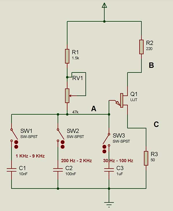
The circuit can be built with the help of few components only and can be built on breadboard also. Here is the circuit diagram followed by description and working and operation of the circuit.
Description : UJT 2N2646 is used in the circuit along with few other components resistors, capacitors and one pot.
• Base 1 terminal of UJT is connected to Vcc through resistor R2 of 220E
• Base 2 terminal is connected to ground through resistor R3 of 50E
• Emitter terminal is connected to junction of pot RV1 (47 K) and 3 capacitors
• One fix value resistance R1 of 1K5 is connected in series with pot RV1
• 3 capacitors C1, C2 and C3 are connected to emitter through 3 SPST switches
Here is the snap of circuit built on bread board
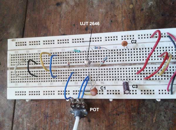
Fig. 1: Prototype of UJT Relaxation Oscillator
Working and operation :
• Give 5 volt supply to the circuit
• When any switch is pressed, that capacitor is connected to pot – emitter junction
• Capacitor start charging to supply voltage
• When it reaches to turn ON voltage of UJT, that is nVBB + VD*, UJT turns ON and capacitor gets discharge path through UJT and resistor
R3
• We can see charging and discharging of capacitor at point A as shown in figure
• When capacitor discharges, it gives a positive spike (very short duration) at base 2 terminal (point C)
• Also when UJT turns ON, base 1 terminal connected to ground so when capacitor discharges and it gives positive spike at base 2, at the
same time on base 1 terminal (point B) it gives negative spike (very short duration)
• The figure given below shows waveforms at point A, B and C
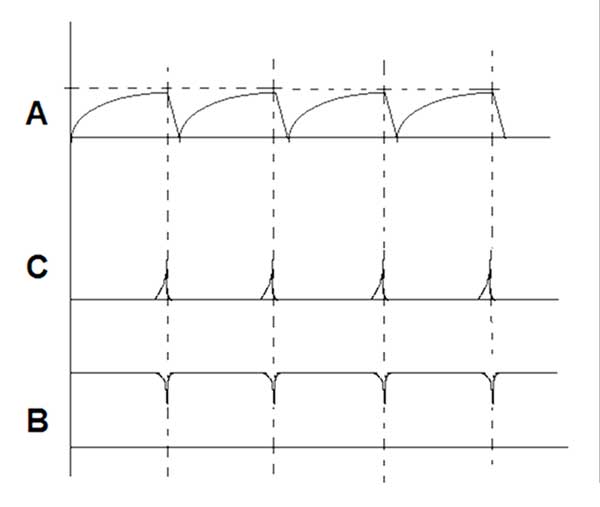
Fig. 2: Signal Diagram of UJT Relaxation Oscillator
• As pot RV1 is varied the charging time and discharging time of capacitor is varied so the frequency of positive and negative spike varies
• Any one capacitor can be selected from given 3 capacitors the will switch the frequency range from Hz to KHz
• Here in this circuit 3 capacitors of 0.01 uF, 0.1 uF and 1 uF are given that will select the frequency range as shown in figure
• The equation for output frequency is
F = 1 / RC ln (1 – n)
where n is intrinsic base ratio and its given by
n = RB1 / (RB1 + RB2)
* to turn on UJT minimum required voltage is nVBB + VD in which
n is intrinsic base ratio and its given by
n = RB1 / (RB1 + RB2)
VBB = supply voltage
VD = internal diode drop between emitter and base 2 terminal
Here are some of snap shots of circuit arrangement, circuit output on DSO at given three different points A, B and C.
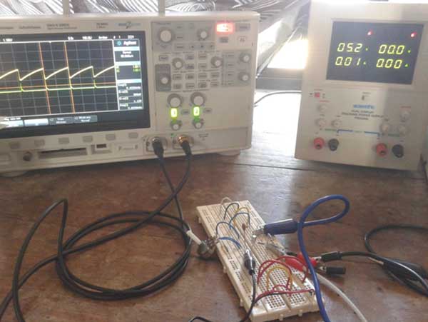
Fig. 3: Image showing UJT Relaxation Oscillator Under Test
The circuit generates different range of frequencies as any one selects different capacitor and the frequency can be varied using given pot.
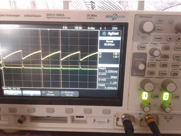
Fig. 4: Image showing Output signal of UJT Relaxation Oscillator observed on CRO

Fig. 5: Image showing Output signal of UJT Relaxation Oscillator observed on CRO

Fig. 6: Image showing Output signal of UJT Relaxation Oscillator observed on CRO
Circuit Diagrams
Filed Under: Electronic Projects


Questions related to this article?
👉Ask and discuss on Electro-Tech-Online.com and EDAboard.com forums.
Tell Us What You Think!!
You must be logged in to post a comment.