CD4027 is a common JK Flip flop based IC and if often used as data storing element. It contains two identical or symmetrical JK flip flop. Individual set of flip flop has provision of pin like set, reset, clock input, J, K and complementary outputs. JK flip flop can be used in applications like registers, counters or as control circuits.
[[wysiwyg_imageupload:7781:]]
Fig. 1: Prototype Of Jk Flip flop Circuit
CD4027 is a master slave JK flip flop IC which works in toggle mode. Here, this IC can be used to change the state by signal applied to one or more control inputs and will have one or two outputs. In this output not only depends upon the current input. A flip flop is mostly used in computer for its memory circuit.
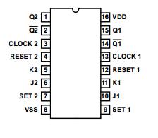
CD4027 has four inputs namely J, K, Set and Reset and it contain two output namely Q and Q bar(Q not) and in this both are opposite of each other. For example voltage on Q bar is zero means Q should be having higher voltage. Output at Q and Q bar depends upon how input is configured. The figure below shows the pin configuration of CD4027 IC:

Fig. 2: Pin Diagram Of CD4027 IC
State of flip flop is controlled by the logic levels present at J and K inputs with some internal controls. Change in state occurs at positive transition of clock pulse. In this, set and reset pin are independent of clock and they are initiated when a high signal is present on any of the input pin.
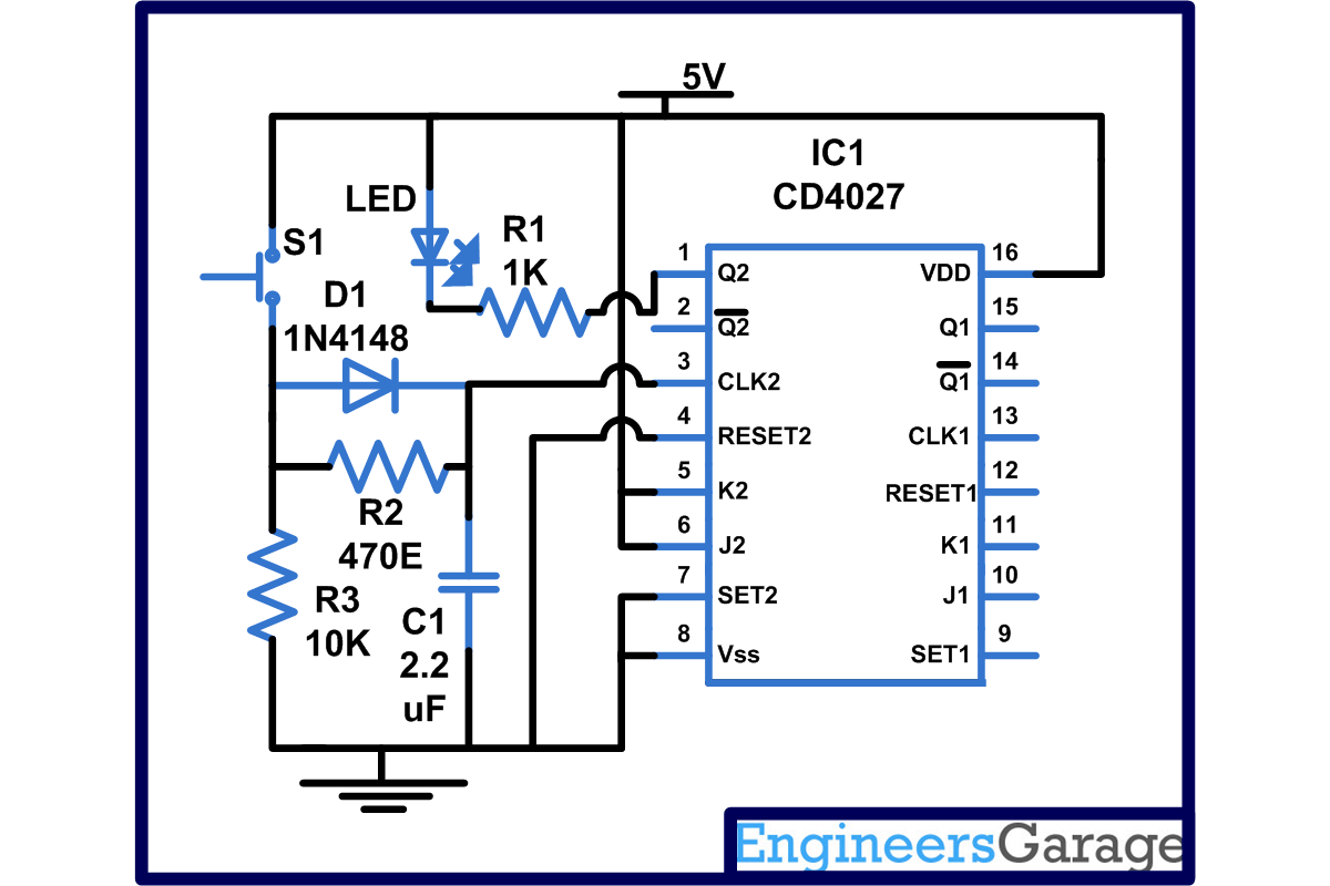
The circuit shown is triggered on the leading edge of the switch, so output changes when switch is once pressed. From the circuit you can see that both J and K are connected to high input means at every negative or positive transition the clock pulse pin 3 toggle between high to low. This can be verified with the help of truth table described below and this stage of flip flop is known as forbidden state.
|
S |
R |
Q |
State |
|
0 |
0 |
Previous State |
No change |
|
0 |
1 |
0 |
Reset |
|
1 |
0 |
1 |
Set |
|
1 |
1 |
? |
Forbidden |
But when you press the switch a short pulse will pass into the clock input of IC which in turn makes the output pin 1 high. The output remains high till the clock input gets the second pulse. This activates the load or LED connected to output. And when this second pulse come on pin 3 the output of IC turn low and load or LED become off.
This circuit works when you press the switch and if you want push to break circuit just interchange the position of switch and resistor.
Circuit Diagrams
Project Components
Project Video
Filed Under: Electronic Projects
Filed Under: Electronic Projects


Questions related to this article?
👉Ask and discuss on Electro-Tech-Online.com and EDAboard.com forums.
Tell Us What You Think!!
You must be logged in to post a comment.