In previous tutorial VHDL tutorial 5, we built NAND, NOR, XOR, and XNOR gates using AND-OR-NOT gates in VHDL.
(If you are not following this VHDL tutorial series one by one, please go through all previous tutorials of these series before going ahead in this tutorial)
In this tutorial,
- We shall write a VHDL program to build a digital circuit to prove De Morgan’s Theorem.
- Verify the output waveform of the program (digital circuit) with the truth table of De Morgan’s Theorem
First, let us see review the statements of De Morgan’s Theorems.
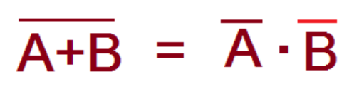
Theorem 1
The complement of the sum of two or more variables is equal to the product of the complement of the variables. Means
Theorem 1
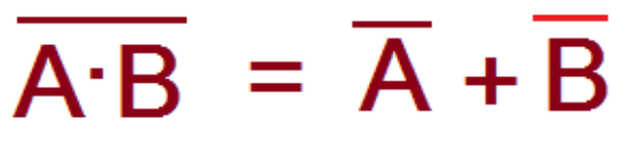
The complement of the product of two or more variables is equal to the sum of the complement of the variables. Means…
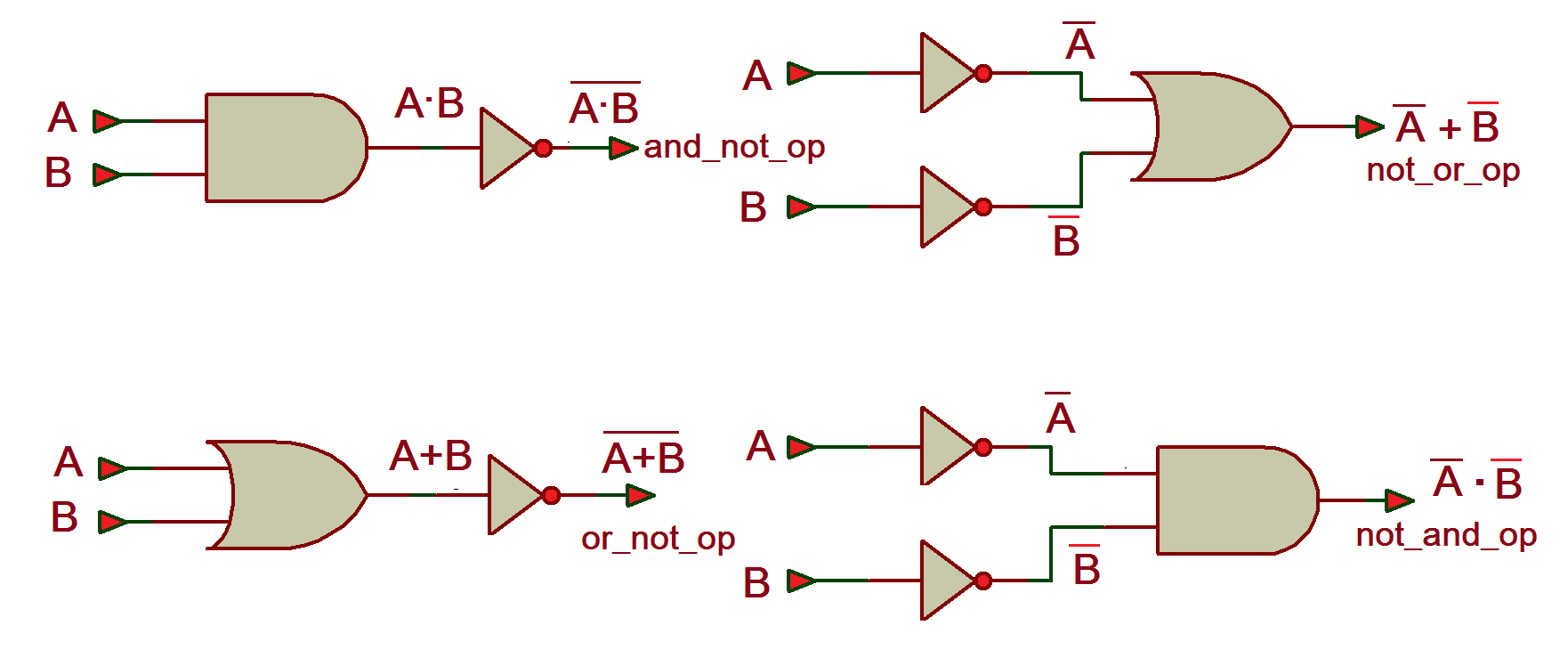
 Let us start with the digital circuit for which we shall write a VHDL program.
Digital Circuit
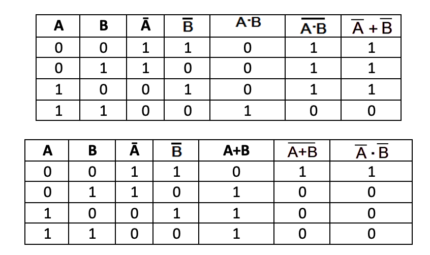
 Here is the truth table for the above circuits.
Now we shall write a VHDL program, compile it, simulate it, and get the output in the form of a waveform. Finely, we shall verify those output waveforms with a given truth table.
(Please go through step by step procedure given in VHDL-tutorial 3 to create a project, edit and compile the program, create a waveform file, simulate the program, and generate output waveforms.)
VHDL Program
library IEEE;
use IEEE.STD_LOGIC_1164.ALL;
entity DMorgan_ckt is
Port (a,b : in std_logic;
and_not_op,not_or_op,or_not_op,not_and_op : out std_logic
);
end DMorgan_ckt;
architecture DMorgan_arch of DMorgan_ckt is
begin
and_not_op <= not (a and b);
not_or_op <= (not a) or (not b);
or_not_op <= not (a or b);
not_and_op <= (not a) and (not b);
end DMorgan_arch;
“entity” describes input-output connections of a digital circuit. As per our circuit given above, we have only two inputs ‘A’ and ‘B’ and four outputs for four circuits.
“architecture” describes the operation of the circuit – means how the output is generated from a given input.
(To know more and get more details about VHDL program(s), please go through the first two tutorials VHDL tutorial 1 and VHDL tutorial 2 of these series.)
Next, compile the above program – create a waveform file with all inputs and outputs listed – simulate the project, and you will get the following result:
Simulation Waveform
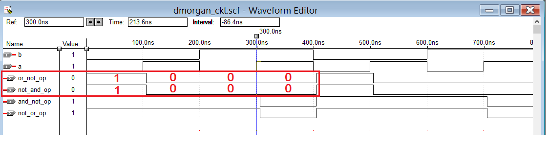 From these output waveforms, we can easily say that the output of OR+NOT is the same as NOT+AND. It is highlighted in the figure. The other two outputs are also the same.
That means De Morgan’s theorems are proven.
In the next tutorial, we shall prove the NAND gate as a universal gate by designing AND, OR, NOT, XOR, and XNOR gates using only NAND gate.
You may also like:


Filed Under: Tutorials, VHDL, VHDL

Questions related to this article?
👉Ask and discuss on Electro-Tech-Online.com and EDAboard.com forums.
Tell Us What You Think!!
You must be logged in to post a comment.