Note: it’s recommended to follow this VHDL tutorial series in order, starting with the first tutorial.
In the previous tutorial VHDL Tutorial – 9, we learned how to build digital circuits from given Boolean equations.
In this tutorial, we will:
- Write a VHDL program to build half and full-adder circuits.
- Verify the output waveform of the program (digital circuit) with the half and full-adder circuits’ truth tables.
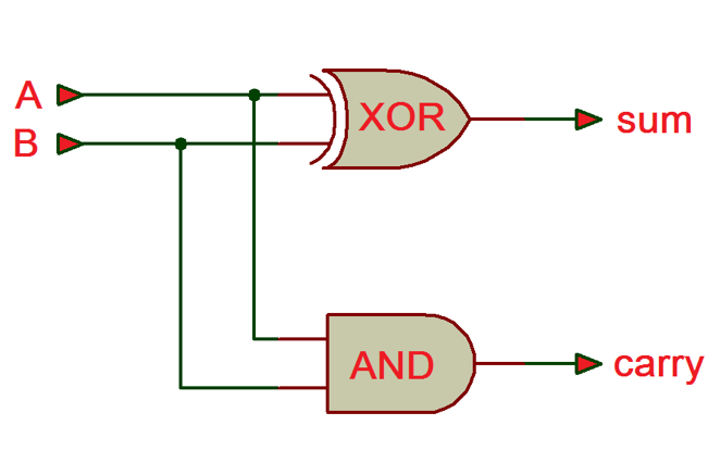
Half-adder circuit
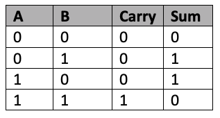
Truth table
Now, we’ll write a VHDL program, compile and simulate it, and get the output in a waveform. We’ll also verify the output waveforms with the given truth table.
However, first it’s important to review the step-by-step procedure provided in VHDL Tutorial – 3. In that tutorial, we learn how to design a project, edit and compile a program, create a waveform file, simulate the program, and generate the final output waveforms.
VHDL program
library IEEE;
use IEEE.STD_LOGIC_1164.ALL;
entity half_adder is
port ( a,b : in std_logic;
sum,cry: out std_logic
);
end half_adder;
architecture adder_arch of half_adder is
begin
sum <= a xor b;
cry <= a and b;
end adder_arch;
Note:
- “entity” describes the input-output connections of the digital circuit. As per the circuit given above, we have two inputs ‘a,’ ‘b,’ and two outputs, ‘sum’ and ‘cry.’
- “architecture” describes the operation of the circuit, which refers to how the output is generated from the given input.
To refresh your memory about how this works, go through the first two VHDL tutorials (1 and 2) of this series.
Next, compile the above program, creating a waveform file with all of the necessary inputs and outputs that are listed, and simulate the project.
Simulation waveform

Verify the ‘sum’ and ‘cry’ output waveforms with the given truth table. For the a=1 and b=0 inputs, the outputs are sum=1 and cry=0, which are highlighted in the figure.
Next, let’s move on to the full adder circuit and its design.
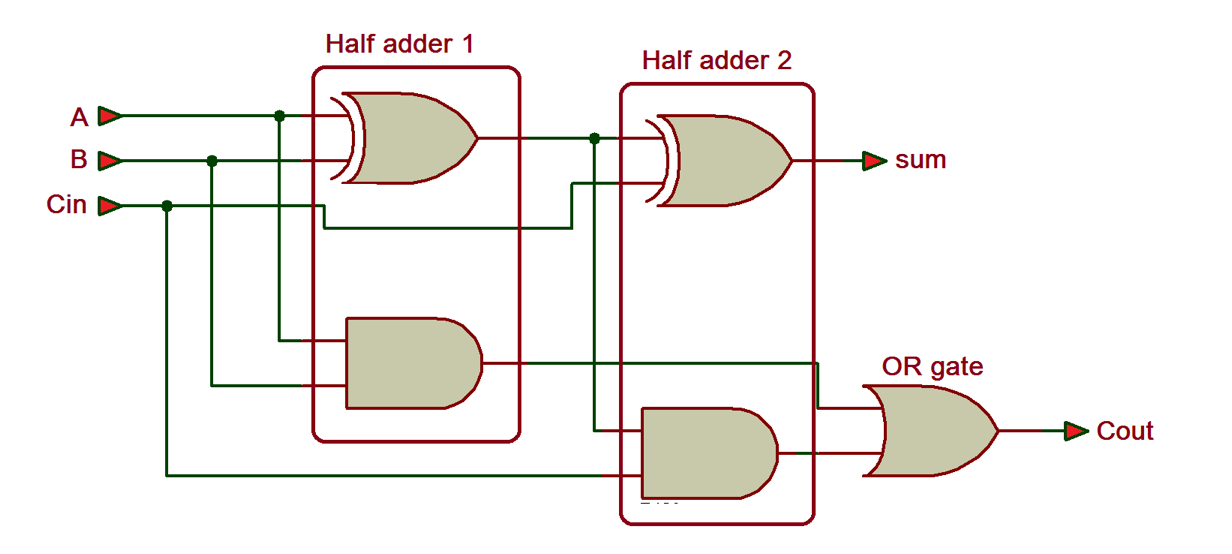
Full-adder circuit
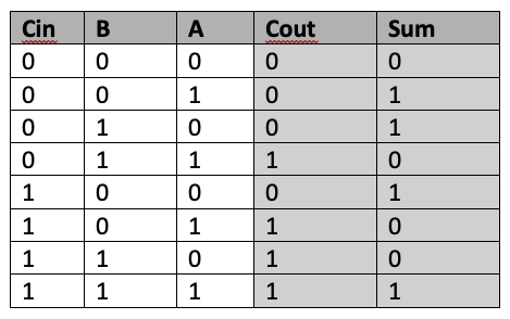
Truth table
Let’s write a VHDL program for this circuit. In the previous tutorial, we designed one Boolean equation digital circuit using a structural-modeling style of the VHDL programming.
Here, we’ll also use that style rather than the data-flow modeling style. We’ll build a full-adder circuit using the “half-adder circuit” and the “OR gate” as components or blocks. (The full-adder circuit consist of two half adder and one OR gate).
VHDL program
library IEEE;
Use IEEE. STD_LOGIC_1164.all;
entity fulladder IS
port (a,b,cin :in STD_LOGIC;
sum,carry : out STD_LOGIC);
end fulladder;
——————————architecture of full adder——————-
architecture FA_arch of fulladder is
—————————–half adder component————————–
component half_adder is
port (p,q :in STD_LOGIC;
s,cy: out STD_LOGIC);
end component;
———————or gate component————————-
component or_gate is
port (p1,q1 :in STD_LOGIC;
r1: out STD_LOGIC);
end component;
——————————-
signal s1,c1,c2 : STD_LOGIC;
begin
w1: half_adder port map (a,b,s1,c1);
w2: half_adder port map (s1,cin,sum,c2);
w3: or_gate port map (c1,c2,carry);
end FA_arch;
————————– half adder program —————————–
library IEEE;
Use IEEE. STD_LOGIC_1164.all;
entity half_adder is
port (p,q : in STD_LOGIC;
s,cy : out STD_LOGIC);
end half_adder;
architecture HA_arch of half_adder IS
begin
s <= p xor q;
cy <= p and q;
end HA_arch;
—————————–or gate program——————————
library IEEE;
Use IEEE. STD_LOGIC_1164.all;
entity or_gate is
port (p1,q1:in STD_LOGIC;
r1: out STD_LOGIC);
end or_gate;
architecture or_g of or_gate IS
begin
r1 <= p1 or q1;
end or_g;
Simulation waveforms
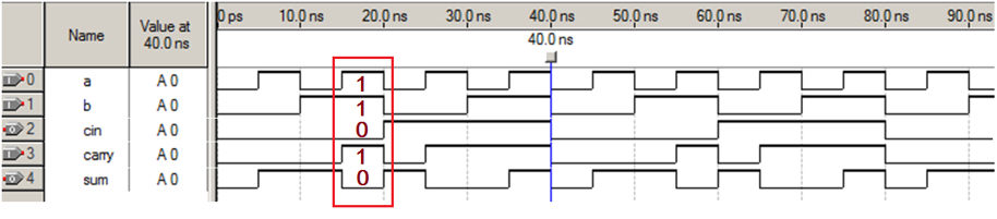
Compare the outputs “sum” and “carry” with the given truth table. In the above figure, one case is highlighted as a=1, b=1, and cin=0, with the outputs of sum=0 and carry=1.
In the next tutorial, we’ll learn how to design half and full subtractor circuits using VHDL.
You may also like:


Filed Under: Tutorials, VHDL, VHDL

Questions related to this article?
👉Ask and discuss on EDAboard.com and Electro-Tech-Online.com forums.
Tell Us What You Think!!
You must be logged in to post a comment.