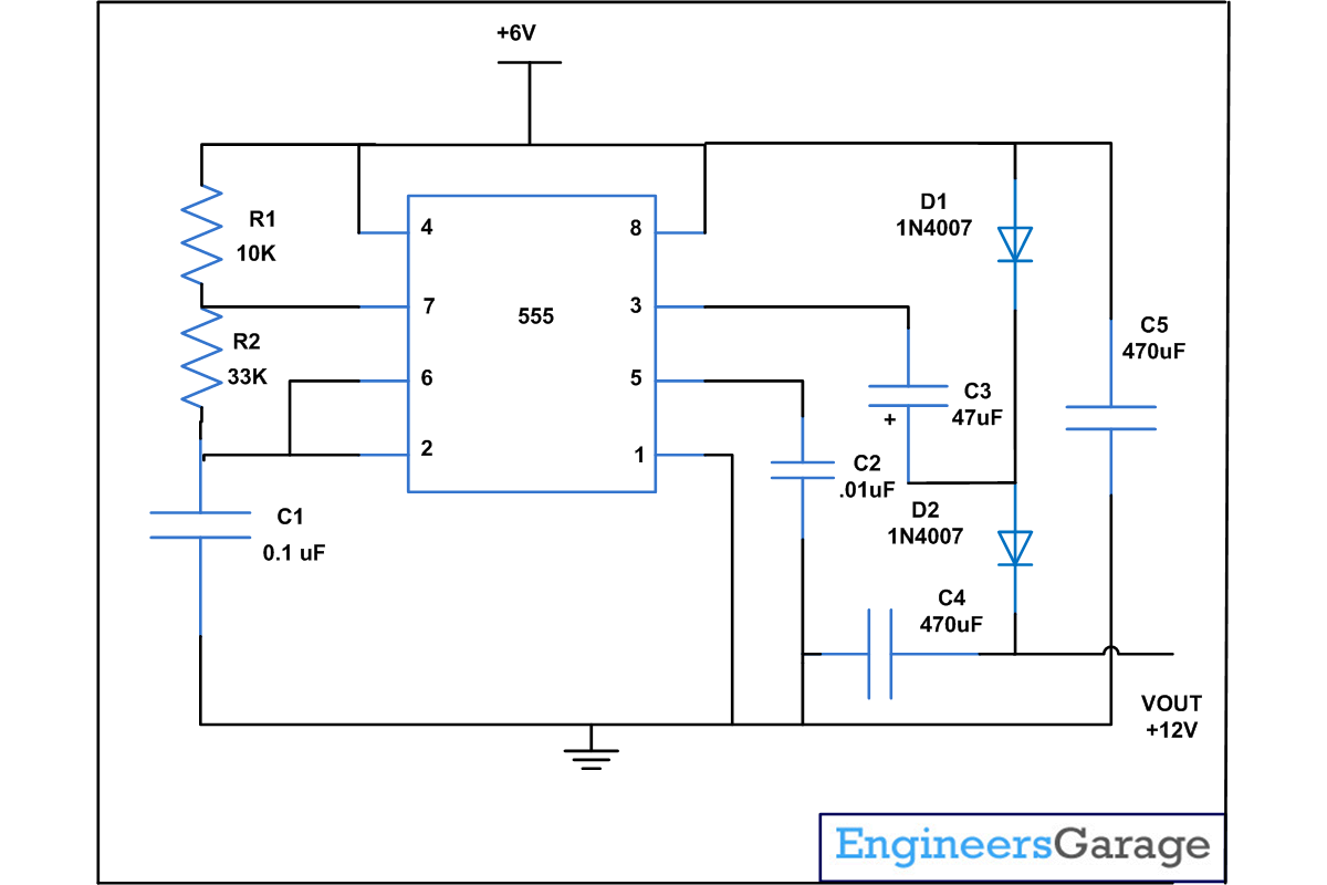
Most of this project is circuit used for doubling the voltage uses the principle of charging and discharging the capacitor. The voltage doubler circuit described below is used to double the input DC power by using IC 555 timer with capacitors and diodes. This circuit is useful when higher voltage level is required from a single lower voltage power supply.
This voltage doubler project is based on 555 timer wired in astable mode means it will produce a square wave at a frequency of 2KHz approx with the help of components R1,R2 and C1.When input power is supplied to the circuit an output is produced at PIN3 of IC1.
Here capacitor C3 and diode D2 are connected in forward biased condition and used to amplify the signals. Diode D1 is used to protect the C3 from complete discharge. The following capacitor C4 therefore gets charged with a combined voltage from C3 and power supply. Therefore in this circuit, components like C3, C4, D1 and D2 are used to boost the input power.
A supply voltage of 3V to 12 V can be given to the circuit and not more than this. If the limit is exceeded then it will destroy the NE555 IC. 1N4148 diode can also be used in the place of 1N4007 but output voltage will decrease because breakdown voltage points of both the diodes differ.
Circuit Diagrams
Project Components
Filed Under: 555 Timers, Electronic Projects


Questions related to this article?
👉Ask and discuss on Electro-Tech-Online.com and EDAboard.com forums.
Tell Us What You Think!!
You must be logged in to post a comment.