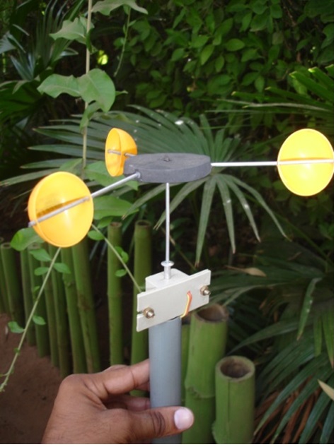
Fig. 1: Block Diagram of Transmitter Unit of Scada based Wireless Anemometer
The block diagram shows the various parts that are included in the Transmitter Part. The transmitter is divided into 5 parts:

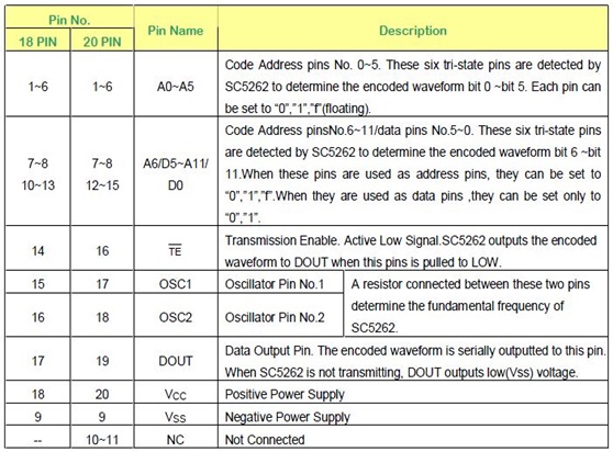
Fig. 2: Pin Diagram of SC5262 IC

|
9 address bits
|
3 Data bits
|
Sync. Bit
|

Fig. 4: Table listing RF Data Bits and Synchronization


Fig. 6: Block Diagram of SC5262 IC

Explanation:
Remote Control Decoder

Fig. 8: Pin Diagram of SC5272 IC
Block Diagram:

Fig. 9: Block Diagram of SC5272 IC

RF Operation for SC5262


Fig. 14: Bit Values of a Code Word


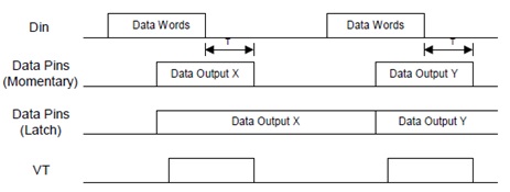
Fig. 17: Signal Diagram for Latch and Momentarily Data Output Type
SCADA Communication Working
During the On time, the connection is made to the SCADA Communication System

Fig. 18: Image showing principle of communication over SCADA
The SCADA will receive the pulses from the transmitter through the SC5272M4. Based on the no. of pulses received in 1 rotation, it will count them and display on the SCADA Screen. This will further calculate the wind velocity of the based on the no. of pulses going in the SCADA. The SCADA need a maximum of 5 volts to operate. So, during the ON time, the connection is made to SCADA and the amplitude of the pulses is kept well below the 5 volt range with help of appropriate resistance.
Hence, SCADA will give us the various parameters like wind velocity, pressure, temperature if appropriate sensors are used. In this case, we have used only the anemometer sensor.
Typical readings of the various parameters that are measured through SCADA are mentioned below:
|
Sr.No.
|
Time
|
Wind Amp (amp)
|
Batt. Volt (volt)
|
H Press. (bar)
|
Temp (c)
|
Velocity
(Kmph)
|
|
|
1
|
00:16
|
0.06
|
23.23
|
1.31
|
28.4
|
21.6
|
|
|
2
|
00:32
|
0.06
|
23.19
|
1.34
|
28.16
|
19.2
|
|
|
3
|
00:49
|
0.06
|
23.2
|
1.37
|
27.92
|
32.8
|
|
|
4
|
01:05
|
0.06
|
23.18
|
1.34
|
27.67
|
20
|
|
|
5
|
01:21
|
0.06
|
23.14
|
1.37
|
27.55
|
18.4
|
|
|
6
|
01:38
|
0.06
|
23.16
|
1.31
|
27.31
|
31.6
|
|
|
7
|
01:54
|
0.06
|
23.16
|
1.31
|
27.19
|
40
|
|
|
8
|
02:10
|
0.06
|
23.14
|
1.37
|
27.07
|
12.8
|
|
|
9
|
02:28
|
0.06
|
23.2
|
1.34
|
26.83
|
16.4
|
|
|
10
|
02:44
|
0.06
|
23.34
|
1.4
|
26.59
|
25.2
|
|
|
11
|
03:01
|
0.06
|
23.44
|
1.34
|
26.35
|
22.8
|
|
|
12
|
03:17
|
0.06
|
23.24
|
1.34
|
26.22
|
20.4
|
|
|
13
|
03:34
|
1.35
|
23.55
|
1.37
|
26.1
|
30.8
|
|
|
14
|
03:50
|
0.06
|
23.23
|
1.28
|
25.86
|
24
|
|
|
15
|
04:06
|
0.06
|
23.14
|
1.34
|
25.74
|
10
|
|
|
16
|
04:23
|
0.06
|
23.16
|
1.37
|
25.5
|
16.4
|
|
|
17
|
04:39
|
0.06
|
23.12
|
1.37
|
25.26
|
21.6
|
|
|
18
|
04:56
|
0.06
|
23.21
|
1.34
|
25.14
|
25.6
|
|
|
19
|
05:12
|
0.06
|
23.16
|
1.4
|
24.9
|
28.4
|
|
|
20
|
05:34
|
0.06
|
23.12
|
1.31
|
24.65
|
14.4
|
|
|
21
|
05:51
|
0.06
|
23.11
|
1.34
|
24.53
|
12.8
|
|
|
22
|
06:07
|
0.06
|
23.09
|
1.31
|
24.29
|
9.2
|
|

Fig. 19: Signal Diagram of Pulse Train at the Receiver


Circuit Diagrams
Filed Under: Electronic Projects


Questions related to this article?
👉Ask and discuss on Electro-Tech-Online.com and EDAboard.com forums.
Tell Us What You Think!!
You must be logged in to post a comment.