
Components
Circuit Diagrams


Working
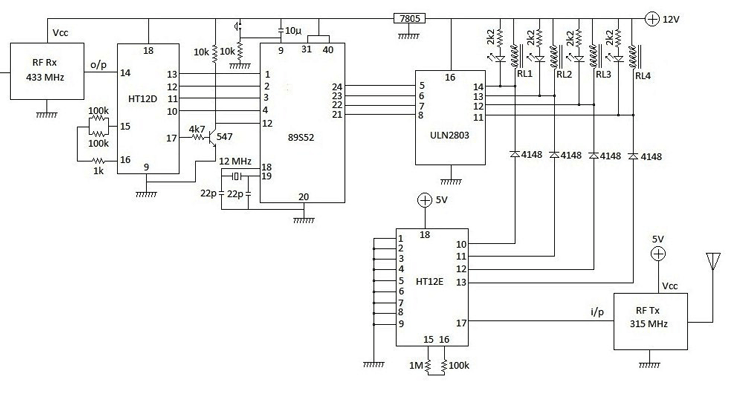
- The rf receiver 1 section
- The decoder 1 section
- The main controller section
- The relay driver section
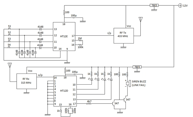
- The feedback encoder 2 section
- The relay based mains switching section
- The rf transmitter 1 and receiver 2 section
- The status display section
- The power supply section
The RF Receiver 1 Section
The Decoder 1 Section
The Main Controller Section
Inductor 2 Section
RF Transmitter 2 & Relay Based Main Switching Section
Power Supply Section
Characteristics & Applications
- This module can be used in any small or big architectural company.
- We can connect many of devices simultaneously with each other & also do on off them automatically or manually.
- We do on off following devices:
Codes
Codes
C code:
Assembly Code:
Project Source Code
Project Source Code
###


 sbit one = P1^0; sbit two = P1^1; sbit three = P1^2; sbit four = P1^3; sbit OP1 = P2^0; sbit OP2 = P2^1; sbit OP3 = P2^2; sbit OP4 = P2^3; //============================================================== void main(void) { TCON = 0x01; IE = 0x81; P1 = 0xff; P2 = 0x00; while(1) { } } //================================================== void EINT0(void) interrupt 0 { if(one == 1) { if(two == 1) { if(three == 1) { if(four == 1) { return; } else { OP4 = ~OP4; } } else { OP3 = ~OP3; } } else { OP2 = ~OP2; } } else { OP1 = ~OP1; } } Assembly Code: org 0000h ljmp main org 0003h ljmp in0 org 0030h main: mov sp,#0fh mov ie,#10000001b setb tcon.0 mov p1,#0ffh mov p2,#00h here: sjmp here in0: jb p1.0,two cpl p2.0 two: jb p1.1,tre cpl p2.1 tre: jb p1.2,four cpl p2.2 four: jb p1.3,next cpl p2.3 next: reti end ###
Circuit Diagrams
Filed Under: Electronic Projects


Questions related to this article?
👉Ask and discuss on Electro-Tech-Online.com and EDAboard.com forums.
Tell Us What You Think!!
You must be logged in to post a comment.