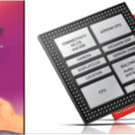
Integrated Circuits rule the world of electronics. Electronic components are available either in discrete or integrated form. The discrete form is reserved for standalone components only, like a transistor, diode, resistor, capacitor, or inductor. It is the ICs that actually made electronics so popular and ubiquitous it is today. All sorts of circuits – analog, digital and mixed-signal, and all types of components – passive or active can be integrated into an IC. You may find very few commercial circuits that may not use any IC.
The ICs, together with other discrete components, are assembled and interconnected on a printed circuit board or a prototyping board to produce an actually functioning electronic circuit. The electronic components come in a variety of packaging. The packaging decides a lot of things. The first one is if the component can be used on a prototyping board, PCB, or both. Normally, electronic components are available in multiple IC packages to suit different phases of product development (like prototyping and production) and suit different circuit design considerations. The packaging of an IC gets really important when it has to be used on a PCB.
There are many different types of IC packages and different ways of classifying these package types. In this article, we will discuss some basics of IC packaging and the common IC packages.
What is IC packaging?
Integrated Circuit Packaging refers to the encasing of a semiconductor component. The core of any IC are semiconductor wafers that are layered in a complex formation with copper and other materials. The cut and formed mash-up of these semiconductor wafers is called a die. The die has all its components and interconnections fabricated at a microscopic level. In the final stage of IC production, macroscopic electrical contacts are taken out from the die, so the integrated circuit can connect with other components on a PCB. The IC packaging is all about encasing the semiconductor ‘die’ and taking out macroscopic electrical contacts for interconnections on a PCB.
Why is IC packaging important?
The packaging of an integrated circuit is as important as the integrated circuit, the semiconductor device within. The packaging mainly serves three purposes – first, it protects the semiconductor circuit from physical impairment or damage. Secondly, it protects the circuit from corrosion. Finally and most important, it decides how electrical contacts are laid out from the semiconductor device over a PCB. This is an important consideration for both IC designing as well as PCB designing. Like how the connections are organized in an IC, how they are laid out using a standard IC package must be coherent with the application and various use cases of the respective IC.
How are IC packages classified?
There are many IC packages, and most of the ICs come in more than one package. Enough to scare off, all those fancy terms DIP, SIP, SOP, SSOP, TSOP, MSOP, QSOP, SOIC, QFP, TQFP, BGA, etc., are all names different IC packages. To better understand these packages, a good idea is to understand their classification.
First of all, IC packages can be classified according to their mounting style. Mounting style is one of the obvious distinguishing factors in ICs. All IC packages fall into two broad categories by mounting style – through-hole (PTH) and surface-mount (SMT). In through-hole packages, the IC leads are designed to be inserted through holes on the PCB before soldering. PTH was introduced to work with printed circuit boards having tracks on both sides and inner layers. Through-hole packages are bigger and easy to work with. These can be used with breadboards and prototyping boards as well. Though surface-mount technology succeeded plated through-hole (PTH), through-hole is still used in commercial circuits wherever surface-mount is not suitable. For example, for semiconductor components with heat sinks, inductors, and transformers, through-hole mounting is ideal.
In surface-mount packaging, the component is mounted directly on the exterior of the PCB. The components and ICs having surface-mount packaging are called surface-mount devices (SMD). This is a different technology referred to as Surface-Mount Technology (SMT). SMT allows automated placement of more components in a smaller area. The SMD components themselves have smaller form-factor and have either smaller or no leads. SMT has almost overtaken the through-hole packaging. In commercial circuits, the preferred mounting is always SMT except for few situations where through-hole is still the ideal choice.
The second way the IC packages can be further classified is how the pins are laid out of the device. All ICs are linear, rectangular, or square in shape. The pinout can be linear, in two parallel directions, all four sides, or matrix form.
The third way the IC packages can be further classified is their terminal (pin) shape. The leads are possible in different shapes like linear, mutual folding, L-shape, J-shape, electrode bud, needle shape, solder bud, tape/film shape.
A fourth way to distinguish IC packages is by terminal count. There are two-terminal, three-terminal, four-terminal, five-terminal, six-terminal, and more than six-terminal IC packages. The dimensions of the terminals also serve as a distinguishing factor in similar package types.
Broadly, with the above-mentioned criteria, all different IC packages can be easily distinguished. Most of the vendors and IC suppliers provide a tabulation of IC packages by first classifying the packages by the number of terminal rows (single row, dual row, quad row, grid array, and unpackaged), then further ramify the packages by mounting style (through-hole and surface-mount), terminal shape and terminal dimensions sequentially. For example, below is a screenshot of a table of IC packages from an online chip supplier.
Another vendor or manufacturer might use a different scheme. For example, the following is a screenshot of the package line-up from Fujitsu.
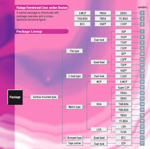
The classification of IC packages by different vendors, suppliers, and manufacturers are done in different schemes. However, the distinguishing factors remain the same as mentioned above. Instead of a tree-structured classification generally used by suppliers and manufacturers, we are listing the major IC package types. These are the following –
- Single in-line
- Zigzag in-line
- Dual in-line
- Quad in-line
- Ceramic flat pack
- Surface-mount small-outline
- Surface-mount leadless
- Flatpack
- Chip carrier
- Chip scale
- Grid Array/Matrix
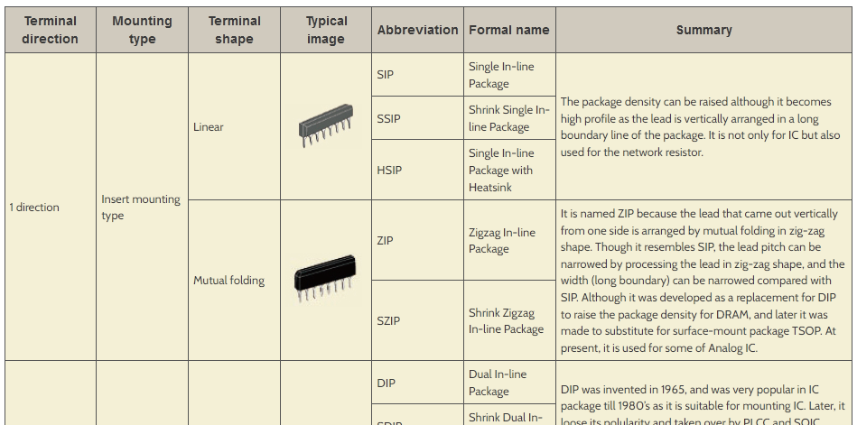
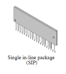
Single inline Packages
These packages have a single row of pins and have a through-hole mounting style. The leads are vertically arranged along the boundary line of the package. Network resistors also use these packages. These packages are useful in reducing the PCB cost by eliminating the need to reduce the wiring pitch. The common single in-line packages are SIP (Single In-line Package), SSIP (Shrink Single In-Line Package), HSIP (Single In-line Package with Heat Sink).
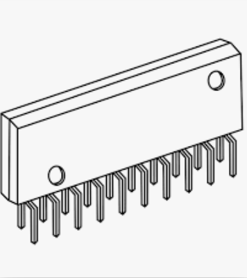
Zigzag Inline Packages
These packages have a single row of pins and have a through-hole mounting style. The leads are vertically arranged along the boundary line of the package, just like SIP but are arranged by mutual folding in zigzag. This package type was introduced to increase the package density of DRAM. At present, it is only used by some analog ICs. The common zigzag inline packages are ZIP (Zigzag In-line Package) and SZIP (Shrink Zigzag In-line Package).
Dual In-line Packages
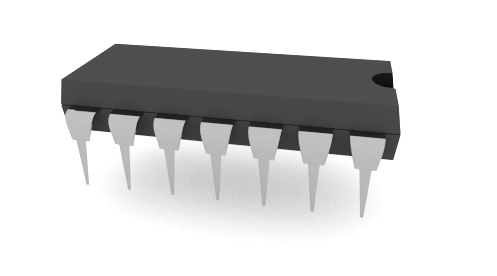
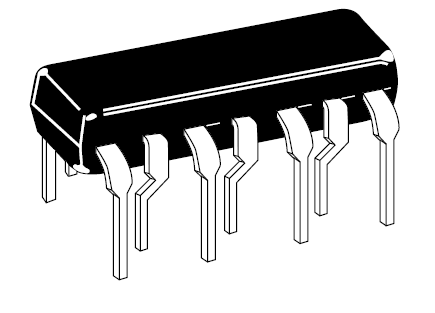
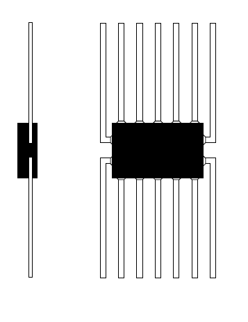
These packages have two rows of pins and have a through-hole mounting style. The leads are arranged in two parallel rows along the package length hanging vertically downwards. This is one of the most popular package styles. Most ICs with 6 to 40 pins have at least DIP as one package type. Though for commercial use, those ICs may be available in surface-mount packages. Dual in-line packages are handy to use on breadboards and prototyping boards. The common dual-inline packages are DIP (Dual In-line Package), SDIP (Shrink Dual In-line), CDIP (Ceramic Dual In-line), CER-DIP (Glass-sealed Ceramic DIP), PDIP (Plastic DIP), SKDIP (Skinny DIP), WDIP (Dual In-line with Window Package), and MDIP (Molded DIP).
Quadruple Inline Package
This package type is similar to DIP except that the leads on two rows are alternatively vertical and zigzag. The common quadruple inline packages are QIP/QIL (Quad In-line) and QUIP (ceramic leadless QIP).
Ceramic Flat Pack
These IC packages have a smaller pitch (50 mils) and were designed for US military standardized PCBs. The leads are arranged horizontally in two or four rows with surface-mount style. Due to smaller pitches, these packages require expensive board processing and finer IC handling. These packages are rarely used in commercial applications due to high PCB costs. The common ceramic flatpack packages are CFP (Ceramic Flat Pack) and QCFP (Quad Ceramic Flat Pack).
Surface Mount Small Outline Packages
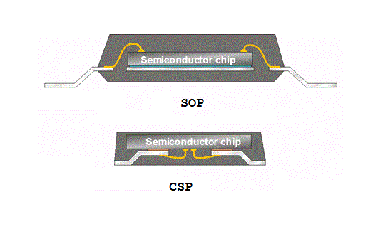
These package types have two rows of terminals and a surface-mount mounting style. The terminals can be L-shape, J-shape, or leadless. SMD components widely use these packages. The J-leaded packages were developed to reduce the space required on the substrate. The leadless types have electrode pads as the terminals for the connections. The common surface-mount small-outline packages are SOP (Small Outline Package), CSOP (Ceramic small-outline package), DSOP (Dual small-outline package), HSOP (Thermally-enhanced small-outline package), SSOP (Shrink Small Outline Package), TSOP (Thin-Small Outline Package), TSSOP (Thin-Shrink Small Outline Package), TVSOP (Thin very-small-outline package), MSOP (Mini/Micro Small Outline Package), HSSOP (Thermally-enhanced shrink small-outline package), HTSSOP (Thermally-enhanced thin shrink small-outline package), QSOP (Quarter Small Outline Package), SOIC (Small Outline Integrated Circuit), mini-SOIC (Mini small-outline integrated circuit), SOICW (Small Outline Integrated Circuit Wide), PSOP (Plastic small-outline package), PSON (Plastic small-outline no-lead package), VSOP (Very-small-outline package), VSSOP (Very-thin shrink small-outline package), SOJ (Small Outline J-leaded package), SON (Small Outline Non-leaded package), VSON (Very-thin Small Outline Non-leaded package), WSON (Very-very-thin small-outline no-lead package), and USON (Very-very-thin small-outline no-lead package).
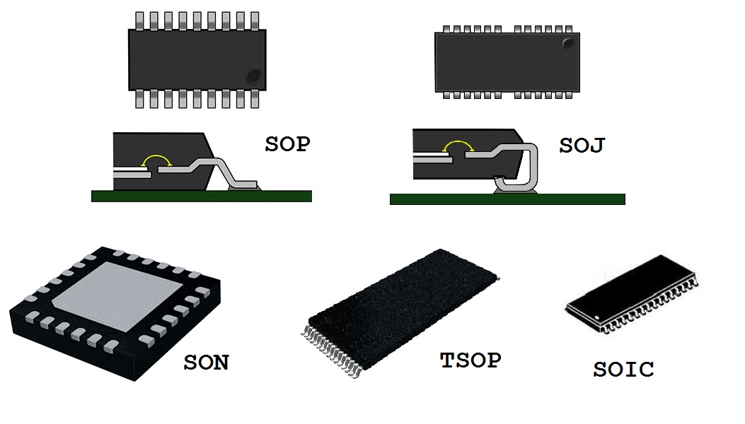
Surface Mount Leadless Packages
These IC packages are the surface-mount type with no leads. The electrode pads along all four edges serve as the terminals for connection. The leadless surface mount packages may also fall into other categories. The common surface-mount leadless packages are LCC (Leadless Chip Carrier), PLCC (Plastic Leaded Chip Carrier), and PQFP (Plastic Quad Flat Pack).
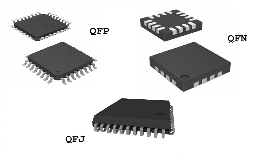
Flat Pack
These IC packages have two or four rows of terminals along the edges of the IC. The mounting style is surface-mount with L-shape, J-shape, or leadless terminals. The common flat pack IC packages are QFP (Quad Flat Package), TQFP (Thin Quad Flat Package), STQFP (Small Thin Quad Plastic Flat Package), FQFP (Fine-pitch Quad Flat Package), HQFP (Quad Flat Package with Heat sink), LQFP (Low profile Quad Flat Package), VQFP (Very-small Quad Flat Package), MQFP (Metric Quad Flat Package), BQFP (Bumper quad flat-pack), ETQFP (Exposed thin quad flat-package), PQFN (Power quad flat-pack), PQFP (Plastic quad flat-package), QFJ (Quad Flat J-leaded package), QFN (Quad Flat Non-leaded package), TQFN (Thin-Quad Flat No-Lead Plastic package), DFN (Dual Flat package), QFI (Quad Flat I-leaded package), HVQFN (Heat-sink very-thin quad flat-pack, no-leads), VQFN (Very-thin quad flat, no-lead), WQFN (Very-very-thin quad flat, no-lead), UQFN (Ultra-thin quad flat-pack, no-lead), and ODFN (Optical dual flat, no-lead).
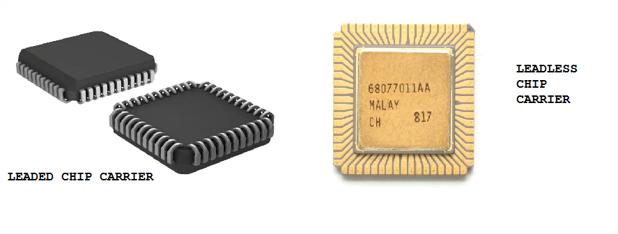
Chip Carrier
These are rectangular IC packages with terminals on all four sides. The terminals are either J-leaded or leadless. The common chip carrier packages are BCC (Bump chip carrier), LCC (Leaded chip carrier), LCCC (Leaded ceramic-chip carrier), PLCC (Plastic leaded chip carrier), LCC (Lead-less chip carrier), CLCC (Ceramic lead-less chip carrier), and DLCC (Dual Lead-less Ceramic Chip Carrier).
Chip Scale/Non-packaged
These IC packages are distinguished because they have almost the same size as the underlying silicon wafer. These are also known as non-packaged ICs. The common chip-scale packages are CSP (Chip-scale package), TCSP (True chip-size package), TDSP (True die-size package), WCSP/WL-CSP/WLCSP (Wafer-level chip-scale package), PMCP (Power mount CSP), Fan-out WLCSP (Fan-out wafer-level packaging), eWLB (Embedded wafer level ball grid array), COB (Chip on board), COF (Chip-on-flex), COG (Chip-on-glass), COW (Chip on wire), TAB (Tape-automated bonding), and MICRO SMD.
Grid Array
These IC packages are square or rectangular in shape and have an array of terminals/pins underneath. The terminals may be through-hole type in needle shape (like PGA (Pin Grid Array), OPGA (Organic pin-grid array), FCPGA (Flip-chip pin-grid array), PAC (Pin array cartridge), CPGA (Ceramic pin-grid array), SPGA (Staggered Pin Grid Array), CGA (Column Grid Array), CCGA (Ceramic Column Grid Array)), surface-mount type with solder ball leads (like BGA (Ball Grid Array), EBGA (Enhanced BGA), eWLB (Embedded wafer level ball grid array), FTBGA (Flex Tape BGA), TFBGA (Thin & Fine-Pitch Ball Grid Array), FBGA (Fine-pitch ball-grid array), LBGA/LFBGA (Low-profile ball-grid array), TEPBGA (Thermally-enhanced plastic ball-grid array), CBGA (Ceramic ball-grid array), OBGA (Organic ball-grid array), TFBGA (Thin fine-pitch ball-grid array), PBGA (Plastic ball-grid array), MAP-BGA (Mold array process – ball-grid array), UBGA (Micro ball-grid array), TBGA (Thin ball-grid array), SBGA (Super ball-grid array), and UFBGA (Ultra-fine ball-grid array)) or leadless surface-mount having electrode pads (like LGA (Land Grid Array)).
You may also like:


Filed Under: What Is

Questions related to this article?
👉Ask and discuss on Electro-Tech-Online.com and EDAboard.com forums.
Tell Us What You Think!!
You must be logged in to post a comment.