The power supplies are the mainstay of electronic circuits. The power supply circuits can be designed in many ways. There can be adjustable power supplies or can be fixed voltage power supplies. A power supply circuit is rated by the voltage or range of voltage it supplies and the maximum current it allows to draw by a load. Secondly, the households are provided with AC voltages as main supplies. A lot of electrical appliances like fans, fluorescent tubes, and others are capable of using AC voltages directly but most of the electronic devices require conversion of AC voltage to DC voltages for their operation. Any external power supply circuit needs to convert AC voltage to DC voltage for use by the electronic devices. In this project, an adjustable power supply circuit is designed which inputs AC mains and provides 0 to 30V 2A DC Voltage as output.
The power supply designed in this project is an adjustable linear regulated type so the output voltage of the circuit is constant and is varied mechanically with the help of a variable resistor. In this type of supply, a linear regulator element (a variable resistor) in series with the load is connected to the output. A linear element like BJT or FET is used to provide required currents at the output.
In the power supply circuit designed here, Bipolar Junction Transistor 2N3055 works in the linear mode along with a variable resistance. The variable resistance helps in providing the appropriate voltage at the output for any current under operating range. The loads powered through the circuit can have different power ratings. High power rating loads draw higher currents. In this power supply circuit, 2N3055 transistor helps in increasing the output current of the power supply to a limit up to 2 A.
The design of a power supply circuit is a step by step process involving stepping down AC voltage, converting AC voltage to DC voltage, Smoothing DC voltage, Compensating transient currents, Voltage regulation, Voltage variation and Current amplification and Short circuit protection.
Components Required –

Fig. 1: List of Components required for Adjustable 0 to 30V 2A DC Power Supply
Block Diagram –

Fig. 2: Block Diagram of Adjustable 0 to 30V 2A DC Power Supply
Circuit Connections –
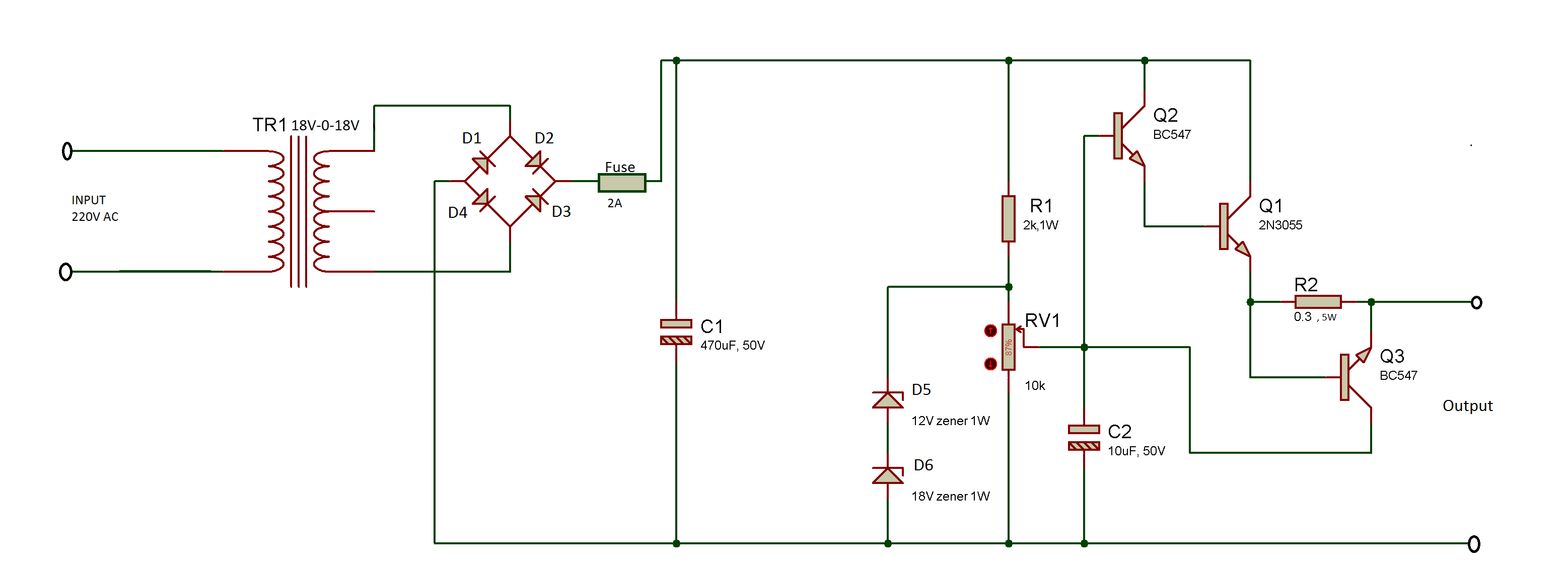
The circuit is assembled in stages with each stage serving a specific purpose. For stepping down the 230 V AC, an 18 V – 0 – 18 V transformer is taken. The secondary coil of the transformer is connected with a full-bridge rectifier. The full bridge rectifier is built by connecting four SR560 diodes to each other designated as D1, D2, D3 and D4 in the schematics. The cathode of D1 and anode of D2 is connected to one of the secondary coil and cathodes of D4 and anode of D3 is connected to other ends of the secondary coil. The cathodes of D2 and D3 are connected from which one terminal is taken out from output of rectifier and anodes of D1 and D4 are connected from which other terminal is taken out from the output from full-wave rectifier. A 2A fuse is connected in series to the output terminal at D2-D3 cathode junctions for safety.
A capacitor of 470 uF (shown as C1 in schematics) is connected between the output terminals of the full-wave rectifier for smoothing purpose. For voltage regulation two zener diodes of 12V and 18V rating are connected in series parallel to the smoothing capacitor. A variable resistance is connected in series to the zener diodes for voltage adjustment and a capacitor of 10 uF (shown as C1 in schematics) is connected in parallel for compensating transient currents. Two NPN transistors (shown as Q1 and Q2 in schematics) are connected as Darlington pair amplifier at one of the output terminals in series to achieve desired current gains. The output of Darlington pair is further connected to an NPN transistor (shown as Q3 in schematics) and resistance (shown as R3 in schematics) for short circuit protection.
Get the schematic diagram drawn or printed on a paper and make each connection carefully. Only after checking each connection made correctly, plug in the power circuit to an AC supply.
How the project works –
The power circuit operates in well-defined stages with each stage serving a specific purpose. The circuit operates in the following stages –
1. AC to AC Conversion
2. AC to DC Conversion – Full Wave Rectification
3. Smoothing
4. Compensation of Transient Current
5. Voltage Regulation
6. Voltage Adjustment
7. Current Amplification
8. Short Circuit Protection
AC to AC Conversion
The voltage of Main Supplies (Electricity fed by the intermediate transformer after stepping down line voltage from generating station) is approximately 220-230V AC which further needs to be stepped down to 30V level. To reduce the 220V AC to 30V AC, a step-down transformer is used.
The circuit takes some drop in the output voltage due to resistive loss. Therefore a transformer of high voltage rating greater than the required 30 V needs to be taken. The transformer should provide 2A current at the output. The most suitable step-down transformer that meets the mentioned voltage and current requirements is 18V-0-18V/2A. This transformer step downs the main line voltage to 36V AC, as shown in the below image.

Fig. 3: Circuit Diagram of 18-0-18V Transformer
AC to DC Conversion-Full Wave Rectification
The stepped down AC voltage needs to be converted to DC voltage through rectification. The rectification is the process of converting AC voltage to DC voltage. There are two ways to convert an AC signal to the DC one. One is half wave rectification and another is full wave rectification. In this circuit, a full-wave bridge rectifier is used for converting the 36V AC to 36V DC. The full wave rectification is more efficient than half wave rectification since it provides complete use of both the negative and positive sides of AC signal. In full wave bridge rectifier configuration, four diodes are connected in such a way that current flows through them in only one direction resulting in a DC signal at the output. During full wave rectification, at a time two diodes become forward biased and another two diodes get reverse biased.

Fig. 4: Circuit Diagram of Full Wave Rectifier
During the positive half cycle of the supply, diodes D2 and D4 conduct in series while diodes D1 and D3 are reverse biased and the current flows through the output terminal passing through D2, output terminal and the D4. During the negative half cycle of the supply, diodes D1 and D3 conduct in series, but diodes D1 and D2 are reverse biased and the current flow through D3, output terminal and the D1. The direction of current both ways through the output terminal in both conditions remain the same.

Fig. 5: Circuit Diagram showing positive cycle of Full Wave Rectifier

Fig. 6: Circuit Diagram showing negative cycle of Full Wave Rectifier
The SR560 diodes are chosen to build the full wave rectifier because they have the maximum (average) forward current rating of 2A and in reverse biased condition, they can sustain peak inverse voltage up to 36V. That is why SR560 diodes are used in this project for full wave rectification.
Smoothing
As the name suggests it is the process of smoothing or filtering the DC signal by using a capacitor. The output of the full-wave rectifier is not a steady DC voltage. The output of the rectifier has double the frequency of main supplies but still containing ripples. Therefore, it needs to be smoothed by connecting a capacitor in parallel to the output of full wave rectifier. The capacitor charges and discharges during a cycle giving a steady DC voltage as an output. So, a capacitor (shown as C1 in schematics) of high value is connected to the output of rectifier circuit. As the DC which is to be rectified by the rectifier circuit has many AC spikes and unwanted ripples, so to reduce these spikes capacitor is used. This capacitor acts as a filtering capacitor which bypasses all the AC through it to ground. At the output, the mean DC voltage left is smoother and ripple free.

Fig. 7: Circuit Diagram of Smoothing Capacitor
Compensating Transient Currents
At the output terminals of the power circuit, a capacitor ( shown as C2 in schematics) is also connected in parallel. This capacitor helps in fast response to load transients. Whenever the output loads current changes then there is an initial shortage of current, which can be fulfilled by this output capacitor.
The output current variation can be calculated by
Output current ,Iout = C (dV/dt) where
dV = Maximum allowable voltage deviation
dt = Transient response time
Considering dv = 100mV
dt = 100us
In this circuit a capacitor of 10 uF is used so,
C = 10uF
Iout = 10u (0.1/100u)
Iout = 10mA
This way it can be concluded that output capacitor will respond for 10mA current change for a transient response time of 100 us.

Fig. 8: Circuit Diagram of Transient Current Compensator
Voltage Regulation
The power circuit should provide regulated and constant voltage without any fluctuation or variation. For voltage regulation, a linear regulator is needed in the circuit. The aim of using this regulator is to maintain a constant voltage of a desired level at the output.

Fig. 9: Circuit Diagram of Voltage Regulator for Adjustable 0 to 30V 2A DC Power Supply
In this circuit, the maximum voltage at the output should be 30V so a 30V zener diode is perfect for voltage regulation at the output. Here two zener diodes of 12V and 18V are connected in series which provide a total of 30V at the output. A 30V zener diode of 1W rating or a different combination of zener diodes can also be used for getting 30V at the output.
Voltage Adjustment
For adjusting output voltage from 0 to 30V a variable resistor (shown as RV1 in schematics) is connected to the output. The variable probe of RV1 is connected to the collector of the BC547 switching transistor (shown as Q3 in schematics). By varying this resistor the emitter of the switching transistor will provide the varying voltage between 0 and 30V.
Current Amplification
The zener diode can provide current in mill amperes only. Therefore for deriving high load current at the output, some linear element must be connected in series with the load that could draw the required current. This circuit uses an NPN bipolar junction transistor as a linear element. A BC547 transistor (shown as Q2 in the schematics) is used for providing the sufficient base voltage to the NPN Bipolar transistor 2N3055 (shown as Q1 in schematics). The 2N3055 transistor is capable of providing 2A current at the output. The transistors are connected in a Darlington Pair Amplifier configuration to output desired current gains. In Darlington pair configuration, the net current gain is a multiplication of the current gains of the two transistors.
Total current gain (hFE total) = current gain of transistor 1 (hFE t1) x current gain of transistor 2 (hFE t2)
Therefore the current gain of BC547 is 800 and that of 2N3055 is from 20 to 70 so taking an average 50. Then,
Total current gain (hFE total) = 800 * 50 = 40,000
This is sufficient to raise the mille ampere currents to ampere levels.
Short Circuit Protection
For short circuit protection, a BC547 switching transistor (shown as Q3 in schematics) and a resistance shown as R2 in schematics is connected in series before the circuit output.
Testing and Precautions –
The following precautions should be taken while assembling the circuit –
• The current rating of the transformer, bridge rectifier, and transistor must be greater than or equal to the output current requirement. Then only the circuit can provide sufficient current at the output.
• The voltage rating of a step-down transformer should be greater than the maximum required output voltage. This is due to the fact that, circuit takes voltage drop due to some resistive loss. Thus input voltage from transformer must be 2 to 3V greater than the maximum output voltage.
• The capacitor C1 at the output of the rectifier is used to handle mains noise and remove ripples.
• The capacitor C2 at the output terminals of the power circuit helps in handling fast transient changes and noise at the output load. The value of this capacitor depends on the deviation in the voltage, current variations and transient response time of the capacitor used.
• The capacitors used in the circuit must have higher voltage rating than the input voltage. Otherwise, the capacitor will start leaking the current due to the excess voltage at their plates and will burst out.
• The zener diodes used in the circuit must be of 1W rating otherwise, they will get damaged due to heating.
• As the current demand will increase at the output load, the transistor 2N3055 will start heating up. To overcome this problem a proper heat sink must be mounted across it to dissipate the excess heat. Otherwise, the transistor can blow off.
• As the circuit is designed to draw a maximum current of 2A at the output, a fuse of 2A should be connected to the output of the full wave rectifier. This fuse will prevent the circuit for drawing current greater than 2A. For current drawn above 2A, the fuse will blow off first cutting off the input supply from the circuit.
Once the circuit is assembled, it’s time to test it. Plug in the circuit to main supplies and change variable resistance. Take the voltage and current readings at the output terminal of the power circuit using a multimeter. Then connect fixed resistances as load and check the voltage and current readings again.
During testing without load, the output voltage on adjusting variable resistance varied by value between 0.3 V to 30.3 V. Therefore, on calculating error, following error percentage is obtained –
% Error = (Experimental value – Expected value)*100 /Expected value
% Error = (30.3 – 30)*100 / 30
% Error = 1%
When a load is connected at the output the maximum voltage is read 30V. With a load of 1K resistance, the output voltage is read 29.1 V showing a voltage drop of 0.9 V. The output current is measured 29.1 mA so the power dissipation at load of 1k resistance is as follow –
Pout = Iout*Iout*R
Pout = 0.0291*0.0291*1000
Pout = 0.84W
If load Resistance used is 470 ohm then a voltage of 28.9 V is measured showing a voltage drop of 1.1 V and current measured comes out to be 61.4 mA. So the power dissipation at load of 470 ohms is as follow –
Pout = Iout*Iout*R
Pout = 0.0614*0.0614*470
Pout = 1.7W
This circuit can be used as power adapter to support a wide range of electronic applications such as broadcasting, digital cameras, printers, laptops and other portable electronic devices. It can also be used as adjustable DC supply source for electronic devices.
Little Talk on Future Supplies –
In the near future, High Voltage Direct Current (HVDC) can become more popular means of power transmission as the focus on renewable energy is growing. The HVDC is commonly employed for inter-country and underwater power transmissions only. This is done to reduce losses by induced inductance and capacitance over long distances. The resistance, inductance, and capacitance of a wire cannot be practically changed. For power transmission within the country, currently, AC is the preferred method. The Alternating Current is preferred for intra-country power transmission despite losses due to inductance and capacitance because stepping down AC voltage is far cheaper than stepping down DC voltage.
An AC voltage can be easily stepped down with the help of a transformer. So the power that is supplied to the households at present is AC voltage. The generating stations supply high AC voltages to reduce power losses. Like the AC voltage supplied to households is 230 V 50 HZ, then the generating station supplies 2300 V over the transmission wire which is stepped down to 230 V by an intermediate transformer. Possibly, the day HVDC from renewable sources will become a common source of household power supplies, the semiconductor-based power circuits will be used for stepping down and voltage regulation.
You may also like:


Circuit Diagrams
Project Video
Filed Under: Tutorials
Filed Under: Tutorials
