Engineers Garage

  • Electronic Projects & Tutorials
    • Electronic Projects
      • Arduino Projects
      • AVR
      • Raspberry pi
      • ESP8266
      • BeagleBone
      • 8051 Microcontroller
      • ARM
      • PIC Microcontroller
      • STM32
    • Tutorials
      • Audio Electronics
      • Battery Management
      • Brainwave
      • Electric Vehicles
      • EMI/EMC/RFI
      • Hardware Filters
      • IoT tutorials
      • Power Tutorials
      • Python
      • Sensors
      • USB
      • VHDL
    • Circuit Design
    • Project Videos
    • Components
  • Articles
    • Tech Articles
    • Insight
    • Invention Stories
    • How to
    • What Is
  • News
    • Electronic Product News
    • Business News
    • Company/Start-up News
    • DIY Reviews
    • Guest Post
  • Forums
    • EDABoard.com
    • Electro-Tech-Online
    • EG Forum Archive
  • DigiKey Store
    • Cables, Wires
    • Connectors, Interconnect
    • Discrete
    • Electromechanical
    • Embedded Computers
    • Enclosures, Hardware, Office
    • Integrated Circuits (ICs)
    • Isolators
    • LED/Optoelectronics
    • Passive
    • Power, Circuit Protection
    • Programmers
    • RF, Wireless
    • Semiconductors
    • Sensors, Transducers
    • Test Products
    • Tools
  • Learn
    • eBooks/Tech Tips
    • Design Guides
    • Learning Center
    • Tech Toolboxes
    • Webinars & Digital Events
  • Resources
    • Digital Issues
    • EE Training Days
    • LEAP Awards
    • Podcasts
    • Webinars / Digital Events
    • White Papers
    • Engineering Diversity & Inclusion
    • DesignFast
  • Guest Post Guidelines
  • Advertise
  • Subscribe

OLED Display Technology

By Preeti Jain October 31, 2012

During the last two decades, organic light-emitting diodes (OLEDs) have attracted considerable interest owing to their promising applications. They have already made inroads into the displays used for mobiles, PDAs and OLED TVs are also available in the market. Soon, OLEDs will be replacing incandescent and fluorescent lamps.
 
Image Showing a Regular OLED Display Screen
 
 Fig. 1: Image Showing a Regular OLED Display Screen
 
OLEDs, based on electroluminescence, are energy conversion devices. They convert electricityinto light. Electroluminescence is the emission of light from materials in an electric field. In 1960, hole injection into an organic crystal was first observed by Martin Pope and his group in anthracene. Three years later, they also observed electroluminescence (EL) from single crystal anthracene and an impurity-doped one under direct current. Despite the high quantum efieciency obtained with such organic crystals, no applications emerged due to the requirement of high working voltage(above 400 V) for visible emission. Subsequently, Helfrich and Schneider achieved double injection recombination electroluminescence in single crystal anthracene using electron and hole injecting electrodes with voltages reduced to ~60 V for observable emission.
 
In 1987, Van Slyke   and C. Tang from Eastman Kodak developed a novel heterostructure- double layered device containing active “small  molecules”. The two thin-film organic layers independently were responsible for hole and electron transport. The device provided good brightness (>1000 cd/m2), low operating voltages (<10V)  and respectable luminous efficiency (1.5 lm/W), research gained the momentum. Additionally, the device showed rectifier behavior, giving rise to the term OLED (organic light emitting diode). This discovery stimulated explosive development of this field.
 
OLED –WHAT IS OLED?
OLED is an emissive technology; they emit light instead of diffusing or reflecting a secondary source.


OLED is an acronym for Organic Light Emitting Diode. OLED is a self light-emitting technology which consists of a number of semiconducting organic layers sandwiched between two electrodes at least one of them being transparent. Transparent electrode is composed of electric conductive transparent Indium Tin Oxide (ITO) coated glass substrate.
 
Picture Showing Semiconducting Organic Layers of a OLED Screen
  Fig. 2: Picture Showing Semiconducting Organic Layers of a OLED Screen
A simplified device structure is shown in following figure. The device on the left has one transparent electrode and emits light on one side only. The device on the right uses both the electrodes as  transparent ones and it emits light in both top and bottom direction.
 
Diagrammatical Image Showing Simplified Device Structure of OLED Screen

   Fig. 3: Diagrammatical Image Showing Simplified Device Structure of OLED Screen

OLEDs are extremely thin, practically 2- dimensional multi-layer devices. The thickness of all the active layers put together is of the order of a 100 nm. This is extremely useful in space critical applications, such as in aircrafts. Also, these devices can work in subzero temperatures and hence can be significance for military applications as well.
 
OLED devices have no restriction on the size and shape. Every conceivable shape, including flexible ones, can be provided.  The devices can be in form of fibers, and woven to fabrics. They can be bent, rolled into films or it can constitute the surface of spheres. For lighting applications, thin glass substrates can be used.
 

Materials for OLED Polymer based LEDs(PLED)

MATERIALS FOR OLED 


OLEDs consist of multiple layers – Cathode, Election Injection Layer(EIL), Electron Transport Layer(ETL), Emission Layer(EML), Hole Transport Layer(HTL), Hole Injection Layer(HIL) and the anode. The multi-layer structure is shown in the following figure
 
Image Showing Multiple Layers of OLED Screen

 Fig. 4: Image Showing Multiple Layers of OLED Screen

An extremely thin layer of indium tin oxide is used as anode; thin layer is used as it has to be optically transparent.  For cathodes, low work-function metals like Li, Mg, and their alloys with Ag or Al are used.
 
Various types of organic materials are used for the functional layers of OLEDs. Since all emission materials are not good for electron or hole transport, different materials for different functions are used. Also, stability of single material emission layer is not good, dye dopants are used for stabilized OLED emission and color tuning.
 
      ·         Electron Transport Materials
Most prominent OLED material is Alq3 . Not only is it a very good emissive material, it is also a good electron transport material. Another electron transport material used is ADN.
 
      ·         Hole Transport Materials
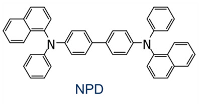
There are several established hole transport materials, but the mature ones are NPD and TPD; both are used in OLEDs.
 
      ·         Dyes
Main purpose of the dyes is – color tuning and color stabilization.
 
Rubrene is used to dope Alq3 for yellow emission.  DCM II and DCJTB are used to dope Alq3 for red emission. C545 is used for green color stabilization and Perlene is used for blue color stabilization.
 
Based on the two classes of electroluminescence materials used in organic light emitting devices, two types of OLEDs are available. Electroluminescence is similar in both types; the difference is in the deposition of the organic films
 

Polymer based LEDs(PLED)

·         Polymer based LEDs(PLED)
Polymers are bigger molecules and hence cannot be thermally deposited. Polymer OLEDs are made by depositing the polymer materials on substrates through inkjet printing process or other solution processing methods(also referred to as ‘wet process’) under ambient conditions. They are used for fabrication of large size screens.
 
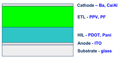
Polymeric OLED devices usually have fewer layers. The electro-active polymers may serve number of functions: some may act as electron transport as well as electon injection and even as emission layer and similarly, some polymers act as hole transport as well as light emission. Dopant emitters are often used for colour tuning. Polymer device structure is shown below. It is bi-layer structure made from solution.ll
 
Various Layers of Polymeric OLED
 
  Fig. 5: Various Layers of Polymeric OLED
Conducting polymers are
.    Polyaniline (PANI:PSS)
.    Polyethylenediooxythiophene(PDOT:PSS)
 
Molecular Structure of Different Conducting Polymers
 Fig. 6: Molecular Structure of Different Conducting Polymers
Emissive polymers are
.   Polyphenylenevinylene (R-PPV)
.   Polyfluorene(PF)
 
Emissive Polymers
  Fig. 7: Emissive Polymers 
·   Small molecule materials (SM-OLED)
Small molecular OLEDs are made by vacuum evaporating (also referred to as ‘dry process’ small molecules to the substrate. Since small molecules do not exhibit any orientating property and therefore form amorphous films.
Small molecular device structure is shown below. It is a multilayer structure made all in vacuum.
 
Image Showing Small Molecular OLEDs Device Structure
   Fig. 8: Image Showing Small Molecular OLEDs Device Structure
Hole Transport small molecules are
.   Metal-phthalocyanines
.   Arylamines, starburst amines
 
Molecular Structure of Hole Transport Small Molecules
    Fig. 9: Molecular Structure of Hole Transport Small Molecules
Emissive small molecules are
.   Metal-chelates, distyrylbenzenes
.   Fluoroscent dyes
 
Emissive Small Molecule
     Fig. 9: Emissive Small Molecule 
 
Transfer material, Emission Layer material and choice of electrode are the key factors that determine the quality of OLED components.
 

OLED – How do OLEDs work?

As explained in previous section, OLED consists of multiple layers; each layer is responsible for a certain function. 


When forward bias is applied on the electrodes, electric fields of the order of 105 – 107  V/cm are generated in the active layers though applied voltages are low, from 2.5 to ~ 20 V.  These high electric fields force charges to be injected across the active layers interfaces. Transparent anode injects the holes while cathode injects the electrons. Sometimes, there is difficulty in injecting carriers into the organic layer from the inorganic contacts. So, to facilitate charge injection, Hole Injection Layer and Electron Injection Layer are used in the structure.
 
Injected holes and electrons from the anode and cathode move inside the material (typically by hopping) and then recombine in the emission layers to form excitons, after which electroluminescence occurs. Radiative relaxation of the excitons generates photons, part of which exit from the transparent side of OLEDs.
The energy level diagram is shown below
 
Energy Level Diagram of OLED Screens
     Fig. 10: Energy Level Diagram of OLED Screens 
Since charge carrier transport relies on hopping process, the conductivity of organic semiconductors is several orders of magnitude lower than that of inorganic counterparts. Also concept of energetic bands is not applicable to organic electronics. Instead of valence and conduction bands, highest occupied and lowest unoccupied molecular orbital (HOMO and LUMO) levels are used.
 
The color of the photon is a function of the energy difference between the HOMO and LUMO levels of the electroluminescent molecule. The wavelength of the light emission can thus be controlled by the extent of the conjugation in the molecule or the polymer.
 
The emission color is a material property. Thus, by stacking several different emitting layers in a single device the total emission can be tuned to virtually every colour including white at any color temperature.
 

OLED Display – Types

OLED DISPLAY – DIFFERENT TYPES OF OLEDS
Displays are often classified as Active Matrix and Passive Matrix and so does the OLED
 

1.      Passive Matrix OLEDs (PMOLED) 


Passive Matrix OLEDs (PMOLEDs) consists of an array of strips of cathode and an array of strips of anode. Sandwitched between the two is the organic layer.  The strips of the anode are arranged at right angles to the cathode strips thereby forming a row and column matrix. Pixels are formed at the intersections of the cathode and anode; the pixels are the points where photons are emitted
 
To illuminate a particular pixel, external circuitry applies current to the row line of anode and column line of the cathode. Thus, the desired pixels can be turned on and off. The brightness of the pixel is governed by the amount of current through the pixel
 
Diagram of Passive Matrix OLEDs

     Fig. 11: Diagram of Passive Matrix OLEDs

Passive matrix OLEDs are relatively low cost and are easier to fabricate. However  they are on the higher side in terms of power consumption when compared with other types of OLEDs due to presence of external circuitry. However, power consumption of   PMOLEDs is smaller than that of LCDs.
 
PMOLEDs can be manufactured economically for small sizes; standard sizes for colour PMOLED are 0.95” and 1.5” and are best suited for small displays of cellphones, PDAs, MP3 players,etc.
 

Active Matrix OLEDs(AMOLED

      2.      Active Matrix OLEDs(AMOLED)


Huge amount of current is required to achieve adequate brightness in passive matrix OLEDs. This necessitates use of large drive voltages leading to increased power dissipation, more flickering and shortened lifetiemes.
 
AMOLEDs uses active matrix addressing, where each pixel is defined by its own electrode and driven by circuitry comprising of thin film transistor and capacitors. The anode is then placed on top of this active-matrix circuitry and the counter electrode, which is not patterned, acts as a ground electrode. In such a device the capacitor is aimed at retaining the information during a frame period.
 
TFT array determines which pixel to turn on or off. By controlling the amount of current through the TFT, brightness is controlled.
 
Active Matrix OLEDs

Fig. 12: Active Matrix OLEDs

AMOLEDs consume lesser power and hence are suited for large displays like TV screens, computer monitors, etc.
OLEDs Displays are also classified as follows
1.      Transparent OLEDs
Transparent OLEDs use transparent anode and cathode as well as transparent substrate.  They can be either passive matrix or active matrix. When turned ON, transparent OLED allows passage of light in both directions.


2.      Top-emitting OLEDs
Top-emitting OLEDs uses either an opaque or reflective substrate. They use active matrix OLEDs
 
3.      Foldable OLEDs


Foldable OLEDs use very flexible substrates such as metallic foils or plastics. Thus they are very lightweight and also durable.

Handheld devices such as cell phones and PDAs find applications of such displays. They can also be sewn into fabrics to form smart clothing.
 
4.      White OLEDs


Compared to fluorescent lights, White OLEDs emit brighter, more uniform and more energy efficient. Like incandescent lights, white OLEDs have true-color qualities.

As OLEDs can be formed into large sheets, they have the potential to replace fluorescent lights used for homes and buildings. Since they consume lesser power, their usage can result in reduced energy costs.
 

OLED –PROS & CONS

OLED –PROS

OLEDs offer numerous advantages over both LCDs and LEDs, including:

.   Thicknes
The organic layers of an OLED are thinner as well as lighter than the crystalline layers used in LCDs and  LEDs. At present, the thickness of OLEDs is less than 2 mm whereas LCD thickness is 4-6 mm. Thickness of OLEDs is likely to go down further.
 
.   Flexibility
As OLEDs use plastic substrate instead of glass (used for LCD), OLEDs can be flexible/foldable.
 
.  Viewing angle
Viewing angles of LCDs have increased significantly to about 170 degrees but at a poor contrast ratio. As LCDs work by blocking light, they have viewing obstacles from certain directions. OLEDs are self emissive, so they have a wider viewing angle. OLEDs are in good approximation Lambertian surface emitter, which means that when viewed from any angle, they have the same apparent radiance.
 
.  Fast Response Time
OLEDs have very response time of the order of tens of microseconds compared to milliseconds for LCDs. This is important for high speed video.
 
·  Power
In LCDs, backlighting consumes lot of power. As OLEDs do not need backlighting, their power consumption is much lesser.  Low power consumption is very useful for energy critical handheld devices like cell phones.
 
.   Emissive technology
OLEDs do not need backlighting, they are self emissive. LCDs functions by selectively blocking areas of the backlight to display the images, while OLEDs light themselves.
 
.   Ease of fabrication
Fabrication of OLEDs is relatively easier. As OLEDs are essentially plastics, they can be formed into thinner and larger sizes. Liquid crystal displays are difficult to grow and lay down.
 
.  Photo-biological Safety
OLED emission is harmless in terms of eye safety. 
 
OLED –CONS 
OLED is probably the perfect technology for the displays; however, they do have some issues, including: 
.  Lifetime: Red OLED and green OLED films have longer lifetimes; typically 10,000 to 40,000 hours. However, blue organics have much shorter lifetimes (around 1000 hours).
.   Manufacturing: Processes are expensive right now.
.   Water: Water can easily damage OLEDs. The organic layers have to be protected against air as they are sensitive to moisture and oxygen and decompose when exposed. Hence they need proper encapsulation
 

OLED Products

OLED PRODUCTS 
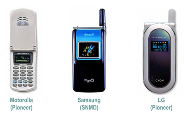
      1.      Small molecule Passive matrix display products 
Image Showing Array of Small Molecule Passive Matrix Display Products
Fig. 13: Image Showing Array of Small Molecule Passive Matrix Display Products
2.      Small molecule Active matrix display products 
Small Molecule Active Matric Display Products

Fig. 14: Small Molecule Active Matric Display Products

      3.      Polymer based Active matrix display products
Polymer based Active Matrix Display Products

     Fig. 15: Polymer based Active Matrix Display Products

      4.      Polymer based Passive matrix display products  
Polymer Based Passive Matrix Display Products

Fig. 16: Polymer Based Passive Matrix Display Products 

OLED –FUTURE

R&D activities in OLEDs is progressing at a fast rate and soon, OLEDs may be visible in heads-up displays(HUD), automotive dashboards, home and office lighting, for flexible displays. Because of the numerous advantages enumerated in previous sections, this will be the technology of choice for displays.

In addition, OLEDs offer several unique features which set them apart from current conventional light sources. They can be very thin, very light weight and they are a non-glaring area light source.  They offer high color quality and turn on instantly when a current is applied. Contrary to usual light sources, OLED lighting modules provide high colour quality that is pleasing to the human eye. They do not contain UV radiation which means they do not bear any risk for eye safety. They have potential to be as efficient and long living or better than fluorescent lamps while 100% mercury-free. All this implies is that OLEDs may go on to become the most efficient light sources in times to come.


Image Showing a Typical Futuristic OLED Screen


Fig.17: Image Showing a Typical Futuristic OLED Screen

OLEDs have the potential to compete with incandescent and fluorescent lighting.  OLEDs will also create new lighting possibilities by enabling large area illumination sources, panels, ceilings, walls, partitions, fabrics etc. OLEDs operate at very low voltages, of the order of 3 – 5 V and therefore, the introduction of OLEDs as sources of light will effect a major paradigm shift in the lighting industry
However, there are still many technical obstacles that have to be overcome before OLEDs become a viable alternative to fluorescent and incandescent lighting.


Filed Under: Articles
Tagged With: lamp, light, oled, pled
 

Next Article

← Previous Article
Next Article →

Questions related to this article?
👉Ask and discuss on EDAboard.com and Electro-Tech-Online.com forums.


Tell Us What You Think!! Cancel reply

You must be logged in to post a comment.

EE TECH TOOLBOX

“ee
Tech Toolbox: Internet of Things
Explore practical strategies for minimizing attack surfaces, managing memory efficiently, and securing firmware. Download now to ensure your IoT implementations remain secure, efficient, and future-ready.

EE Learning Center

EE Learning Center
“engineers
EXPAND YOUR KNOWLEDGE AND STAY CONNECTED
Get the latest info on technologies, tools and strategies for EE professionals.

HAVE A QUESTION?

Have a technical question about an article or other engineering questions? Check out our engineering forums EDABoard.com and Electro-Tech-Online.com where you can get those questions asked and answered by your peers!


RSS EDABOARD.com Discussions

  • Multiple DC/DC converters and a single input source
  • Xiaomi Mijia 1C Robot problem of going backwards while working
  • Will this TL084C based current clamp circuit work?
  • ADS optimization cockpit window does not open
  • Voltage mode pushpull is a nonsense SMPS?

RSS Electro-Tech-Online.com Discussions

  • using a RTC in SF basic
  • Parts required for a personal project
  • Curved lines in PCB design
  • Wideband matching an electrically short bowtie antenna; 50 ohm, 434 MHz
  • PIC KIT 3 not able to program dsPIC

Featured – RPi Python Programming (27 Part)

  • RPi Python Programming 21: The SIM900A AT commands
  • RPi Python Programming 22: Calls & SMS using a SIM900A GSM-GPRS modem
  • RPi Python Programming 23: Interfacing a NEO-6MV2 GPS module with Raspberry Pi
  • RPi Python Programming 24: I2C explained
  • RPi Python Programming 25 – Synchronous serial communication in Raspberry Pi using I2C protocol
  • RPi Python Programming 26 – Interfacing ADXL345 accelerometer sensor with Raspberry Pi

Recent Articles

  • AC-DC power supply extends voltage range to 800 V DC
  • Infineon’s inductive sensor integrates coil system driver, signal conditioning circuits and DSP
  • Arm Cortex-M23 MCU delivers 87.5 µA/MHz active mode
  • STMicroelectronics releases automotive amplifiers with in-play open-load detection
  • Convection-cooled power controller integrates EtherCat connectivity

EE ENGINEERING TRAINING DAYS

engineering

Submit a Guest Post

submit a guest post
Engineers Garage
  • Analog IC TIps
  • Connector Tips
  • Battery Power Tips
  • DesignFast
  • EDABoard Forums
  • EE World Online
  • Electro-Tech-Online Forums
  • EV Engineering
  • Microcontroller Tips
  • Power Electronic Tips
  • Sensor Tips
  • Test and Measurement Tips
  • 5G Technology World
  • Subscribe to our newsletter
  • About Us
  • Contact Us
  • Advertise

Copyright © 2025 WTWH Media LLC. All Rights Reserved. The material on this site may not be reproduced, distributed, transmitted, cached or otherwise used, except with the prior written permission of WTWH Media
Privacy Policy

Search Engineers Garage

  • Electronic Projects & Tutorials
    • Electronic Projects
      • Arduino Projects
      • AVR
      • Raspberry pi
      • ESP8266
      • BeagleBone
      • 8051 Microcontroller
      • ARM
      • PIC Microcontroller
      • STM32
    • Tutorials
      • Audio Electronics
      • Battery Management
      • Brainwave
      • Electric Vehicles
      • EMI/EMC/RFI
      • Hardware Filters
      • IoT tutorials
      • Power Tutorials
      • Python
      • Sensors
      • USB
      • VHDL
    • Circuit Design
    • Project Videos
    • Components
  • Articles
    • Tech Articles
    • Insight
    • Invention Stories
    • How to
    • What Is
  • News
    • Electronic Product News
    • Business News
    • Company/Start-up News
    • DIY Reviews
    • Guest Post
  • Forums
    • EDABoard.com
    • Electro-Tech-Online
    • EG Forum Archive
  • DigiKey Store
    • Cables, Wires
    • Connectors, Interconnect
    • Discrete
    • Electromechanical
    • Embedded Computers
    • Enclosures, Hardware, Office
    • Integrated Circuits (ICs)
    • Isolators
    • LED/Optoelectronics
    • Passive
    • Power, Circuit Protection
    • Programmers
    • RF, Wireless
    • Semiconductors
    • Sensors, Transducers
    • Test Products
    • Tools
  • Learn
    • eBooks/Tech Tips
    • Design Guides
    • Learning Center
    • Tech Toolboxes
    • Webinars & Digital Events
  • Resources
    • Digital Issues
    • EE Training Days
    • LEAP Awards
    • Podcasts
    • Webinars / Digital Events
    • White Papers
    • Engineering Diversity & Inclusion
    • DesignFast
  • Guest Post Guidelines
  • Advertise
  • Subscribe