Timer Registers
TCON (Timer Control register)
TCON is an 8-bit register. Its bits are used for generating interrupts internal or external. The most important bits of the timer TR and TF are also in it. TR (timer run) and TF (timer overflow) bits which we use in almost all over timer applications are in it.
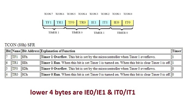
TCON register
- IT0/IT1=> Used for timer Interrupts when IT0/IT1=1 specifies interrupt on falling edge and when IT0/IT1=0 it specifies interrupt on low level
- IE0/IE1=> Used for external Interrupts
- TR0/TR1=> Timer 0/1 run control flag when it is 1 it means timer is running.
- TF0/TF1=> Timer 0/1 overflow flag when it is 1 it means timer is over flow.
TH0/TL0 & TH1/TL1
These two registers TH and TL are timer high byte and timer low byte, 0 and 1 are the timers numbers. They are 16-bit registers. we give our time delays in it. since 8051 is an 8-bit micro controller, we access its register in two bytes one byte for TH(timer high byte) and one for TL(timer low byte).
How to calculate values for TH and TL registers here is an example click on the link below.
www.microcontroller-project.com/internal-timer–registers-of-8051.html
How to calculate values for TH and TL registers here is an example click on the link below.
www.microcontroller-project.com/internal-timer–registers-of-8051.html
TMOD (Timer Mode register)
8-bit register used to select timer mode. There are 4 modes in which timer can be loaded.
1. 13-bit timer
2. 16-bit timer
3. 8-bit auto reload
4. Split timer mode
TH0/TL0->Timer 0 16 bit register (byte addressable only) 8 bits can be send at a time.
TH1/TL1-> Timer 1 16 bit register (byte addressable only) 8 bits can be send at a time.
1. 13-bit timer
2. 16-bit timer
3. 8-bit auto reload
4. Split timer mode
TH0/TL0->Timer 0 16 bit register (byte addressable only) 8 bits can be send at a time.
TH1/TL1-> Timer 1 16 bit register (byte addressable only) 8 bits can be send at a time.
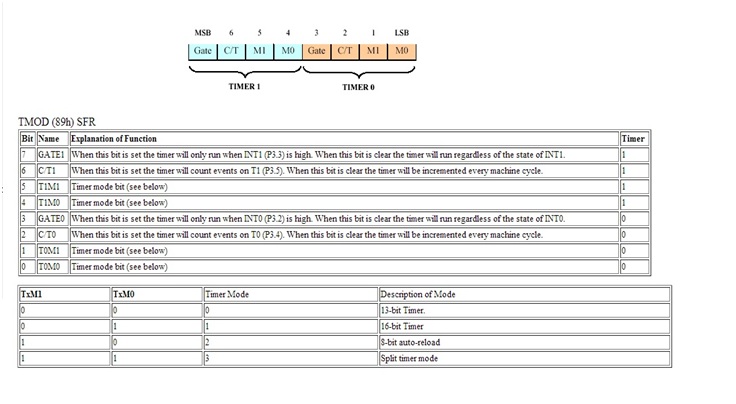
8051 TMOD register
Serial registers
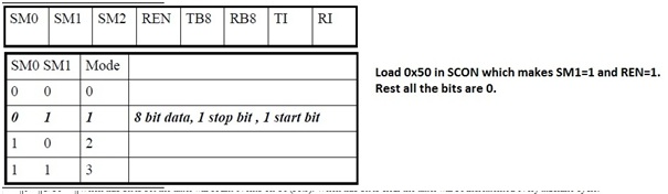
SCON (Serial Control)
It’s an 8 bit register, Used for serial data communication. It is bit addressable.
8051 SCON register
SM0, SM1 and SM2 are used to specify the serial connection mode.
There are five different modes four are shown above in the diagram. The fifth one is when we make SM2=1 which is 8-bit transfer mode. The most common mode is mode 1.
REN is Receive Enable, when REN=1 it allows the 8051 to receive and transfer data . If you want 8051 to both transfer and receive data, REN must be set to ‘1’. when REN=0 it means receiver is disabled.
TB8 and RB8 is used for serial modes 2 and 3.
TI and RI are important bits.
TI is Transmit Interrupt flag, When 8051 micro controller finishs the transfer of 8-bit character, it raises the TI flag to indicate that it is ready to transfer another byte.
RI is Receive Interrupt flag, When 8051 receive data via RxD pin(Port1 pin 0), it get rid of the start and stop bits and places the byte in the SBUF. Then it raises the RI flag to indicate that a byte has been received and should be picked up before it is lost.
SBUFF (Serial Buffer)
This register is used when we are transmitting or receiving data serially. We put or data in it which we want to transmit, it also contains the data which is transmitted from other Peripherals like PC personal computers to 8051 micro controller. It is not bit addressable.
Register Banks
8051 has four Register banks. When the 8051 is first booted up, Register bank 0 (addresses 00h through 07h) is used by default. The internal memory supports 4 register banks. The first 8 bytes (00h – 07h) are “register bank 0”. Followed by Bank1 (08 – 0F), Bank2 (10 – 17), Bank3 (18 – 1F). Register banks reside in the first 32 bytes of Internal RAM.
PSW (PROGRAM STATUS WORD)
This is an 8-BIT register. The Program Status Word (PSW) contains status bits that reflect the current CPU state.
A (ACCUMULATOR)
Accumulator is an 8-bit register.It holds the result of most of arithmetic and logic operations. This register is usually accessed by direct addressing. It is both byte and bit addressable.
B (EXTENSION REGISTER)
The major purpose of B(Extension register) register is executing multiplication and division. This register is directly accessed when we are writing our code in assembly language. The 8051 micro controller has a single instruction for multiplication (MUL) and division (DIV).
SP (STACK POINTER)
Stack pointer is an 8 bit register, the direct address of SP is 81H and it is only byte addressable, which means you cant access individual bits of stack pointer. The content of the stack pointer points to the last stored location of system stack. To store something new in system stack, the SP must be incremented by 1 first and then execute the “store” command.
- Push increments the SP and writes data.
- POP reads data and then decrements the SP.
- Stack is kept in the internal RAM and is restricted to 128 bytes.
- Top most address of stack is 7F.
DPTR (DATA POINTER REGISTER)
This is a 16 bit register. It is used to access external code or data memory
The Data Pointer (DPTR) is the 8051’s only user-accessible 16-bit (2-byte) register.
The Data Pointer (DPTR) is the 8051’s only user-accessible 16-bit (2-byte) register.
PCON(Power Control Register)
PCON is an 8-bit register used to control the baud rate during serial communication and 8051’s power control modes.
● Setup double baud rate when timer1 is used for serial communication in modes 1,2 &3
● Switch to sleep mode on PD Power Down
● Switch to Idle mode when IDL bit is set.
Register bits and Functions
● Setup double baud rate when timer1 is used for serial communication in modes 1,2 &3
● Switch to sleep mode on PD Power Down
● Switch to Idle mode when IDL bit is set.
Register bits and Functions
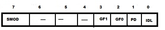
SMOD => Double Baud rate when Serial port is used in mode 1,2 or 3.
GF1 => General purpose flag bit.
GF0 => General purpose flag bit.
PD =>Power down. Activates power down operation.
IDL =>Ideal mode. Activates ideal mode operation.
— => Reserved
Ø In IDL(Ideal) mode internal clock is disconnected from the processor but remains connected to interrupt, timer and serial port functions. IDL mode is terminated on interrupt or system reset.
SFR registers (special function registers)
We can access 8051 ports and all other registers using sfr’s. They are actually the registers locations which are dedicated for each individual port or register etc.
- 8Ch is SFR for TH0 register
- 8Ah is SFR for TL0 register
- 8Dh is SFR for TH1 register
- 8Bh is SFR for TL1 register
- 88h is SFR for TCON register
- 89h is SFR for TMOD register
- 98h is SFR for SCON register
- 99h is SFR for SBUF register
- 80h is SFR for P0 (Port 0 of 8051)
- 90h is SFR for P1 (port 1 of 8051
- A0h is SFR for P2 (port 2 of 8051)
- B0h is SFR for P3 (port 3 of 8051)
- E0h is SFR for ACC (Accumulator register)
- D0h is SFR for PSW (Program status word)
- 81h is SFR for SP (Stack pointer)
- F0h is SFR for B (Extension register)
Filed Under: Knowledge Share, Microcontroller Projects

Questions related to this article?
👉Ask and discuss on Electro-Tech-Online.com and EDAboard.com forums.
Tell Us What You Think!!
You must be logged in to post a comment.