+/- 1.25V to +/-22V 1A Adjustable Power Supply
About Power Supply
The power supply is the mainstay for every electronic device. As the name suggests power supply are power providers for any circuit. Every electronic circuitry needs a proper power supply at the input for its optimum result at the output. We need to choose the power supply of any device or circuit as per the power requirements of the device. In this experiment, we are making an adjustable power supply, which will give voltage in the range of +/- 1.25 V to +/-22V with 1A as maximum current.
Overview
In this experiment, we are making an adjustable regulated symmetrical positive and negative power supply. For reducing any fluctuation and ripples at the output the supply must be regulated so that it can provide a constant voltage at the output. This power supply provides regulated as well as the adjustable voltage at the output.
The supply which we are making takes 220V AC as input and generates a variable DC voltage in the range of +/- 1.25 V to +/-22V. This power supply can provide a maximum current of 1A at the output.
Components required
| Components Name | Specification | Quantity |
|---|---|---|
| Transformer Tr1 | Step down 24 V-0-24V/2A | 1 |
| Diode D1-D6 | 1N4007 | 6 |
| Variable Resistance
RV1, RV2 |
10k | 2 |
| Voltage Regulator | LM317 | 1 |
| Voltage Regulator | LM337 | 1 |
| Capacitor C1, C2 | 100uF 63V | 2 |
| Capacitor c3, c4 | 10uF 63V | 2 |
| Capacitor C5,C6 | 1uF 50V | 2 |
| Ceramic Capcitor C7,C8 | 0.1uF | 2 |
| Resistor R1,R2 | 240 OHM | 2 |
| Fuse | 1A | 2 |
Basics of Power Supply
Every DC power supply needs some steps to follow for getting proper DC voltage at the output. Below diagram shows these basic steps by which we get a regulated DC power supply by AC.

Working
• Step down the Mains supply by input transformer
The voltage of Mains (Electricity which is coming at our home from Govt) is approximately 220V but as per the circuit requirement, only 22V voltage is required at the output terminal. To reduce this 220V to 22V a center tape step-down transformer is used. The use center tap transformer is to generate both positive and negative voltage at the output. The center tape will provide ground to the circuit and remaining two taping will provide positive and negative voltage. The step-down transformer we are using is 24V-0-24V/2A rating. This transformer downs the main line voltage to 24V, as shown in the below image. The circuit takes some drop in the form resistive loss and by the LM317 IC. Therefore a transformer of high voltage rating than the voltage required for the application is taken in the circuit and it can provide 2A current at the output, which is well suited for our 1A application.

• Rectification
The rectification is the process of converting AC to DC. There are two ways to convert an AC signal to DC. One is through half wave rectifier and another is by using a full wave rectifier. In this circuit, we are using a full wave bridge rectifier for converting the +/-24V AC to +/-24V DC. As full wave rectifier is more efficient than a half wave since it can provide complete use of both the negative and positive pulse of AC signal. In full wave bridge rectifier configuration, four diodes are connected in such a way that it generates a DC signal at the output, as shown in below image. The 1N4007 diode is used in full wave rectification as it can allow 1A current and 24V supply.

• Smoothing
As its name suggest it is the process of smoothing or filtering the DC signal by using a capacitor. A capacitor C1 and C2 of high value is connected at the input side after the bridge rectifier to give pure DC at the output. As the DC which is rectified by the rectifier circuit has many AC spikes and ripples so to reduce these spikes we use a capacitor. This capacitor acts as a filtering capacitor which bypasses all the AC through it to ground. At the output, the DC which is left is now smoother and ripple free.

• Output capacitor
At the output, capacitor C5, C6, C7 and C8 are also connected to the circuit. The capacitor C5 and C6 helps in fast response to load transients. Whenever the output load current changes then there is an initial shortage of current, which can be fulfilled by this output capacitor.
The capacitor C7 and C8 are ceramic capacitors, the impedance or ESR of ceramic is low as compared to an electrolytic capacitor. Therefore C7 and C8 are used in parallel to electrolytic capacitor just to decrease the equivalent output impedance.

The output current variation can be calculated by – :
Output current ,Iout = C (dV/dt)
dV = Maximum allowable voltage deviation
Consider dv = 100mV
By this, we can say output capacitor will respond for 1mA current change for a transient response time of 100us .At adjustment pin capacitor C3 and C4 are connected. These capacitors prevent the ripple to be amplified as the output voltage is increased.
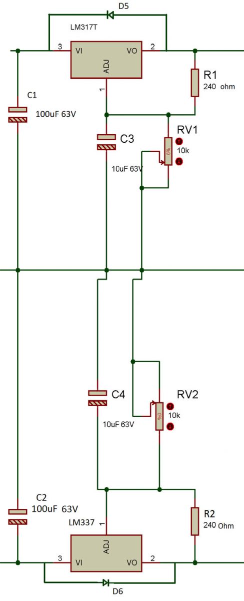
• Voltage regulation by LM317
For providing a regulated 1.25V to 22V LM317 IC is used and for -1.25 to -22V at the output LM337 IC is used. Both the IC are capable of providing current of 1.5A, thus well suited for our requirements of 1A. In this circuit, LM317 and LM337 will provide an adjustable voltage corresponding to its input voltage. Both of them have the good feature of load regulation. They will provide regulated and stabilized the voltage at the output irrespective of the variation in the input voltage and load current.
About LM317 and LM337
317 is a positive voltage regulator which gives output in the range of 1.25V to 37V with input voltage up to 40V. Contrariwise 337 is a negative voltage regulator which will provide -1.25V to -37V with input voltage up to -40V. At the output both can provide a maximum current of 1.5A as per the datasheet under the optimum condition.
For setting a desired voltage at the output resistive voltage divider circuit is used between the output pin and ground. The voltage divider circuit has one programming resistor (fixed resistor) and another is a variable resistor .By taking a perfect ratio of feedback resistor (fixed resistor) and variable resistor we can obtain desired value of output voltage corresponding to the input voltage.
In this experiment, the R1 and R2 resistance are used as a programming resistance for 317 and 337 respectively.
The variable resistance RV1 and RV2 are used to vary the output voltage at 317 and 337 respectively.
• Protection diode
A diode D5 should be connected to the 317, as in below image. So that it can prevent the external capacitor from discharging through the IC during an input short circuit. When the input is shorted then the cathode of the diode is at ground potential. The anode terminal of the diode is at high voltage since C5 is fully charged. Therefore in this case diode is forward bias and all the discharging current from capacitor passes through a diode to ground. This will save the LM317 from the back current.
In a similar way, a diode D6 is connected with the 337 IC to prevent the IC from discharging of the capacitor C6 through the IC when the input is shorted.

• Output voltage
The output voltage can vary by using the adjust pin of 317 and 337. The variable resistor RV1 and RV2 provide the output voltage from 1.25V to 22V and -1.25 to -22V respectively.
Practical Observation
Output voltage without load
• At LM317
By varying RV1 we can vary the output voltage in the range of
• Load RL1 = 50 ohm
Then output current
I out = 300mA
By varying RV2 we can vary the output voltage in the range of
Vout = -1.25V to -22V
When load is connected at the output by setting the voltage at -20V
• Load RL1 = 50 ohm
Vout (Observed) = 17.5V(voltage drop from -20V to -17.5V)
Then output current
I out = 320mA
By this, it can be analyzed that when current demand increases at the output then the output voltage will start reducing. As the current demand increases then 317 and 337 IC start heating up and IC will take more drop across it which will reduce the output voltage. Hence a proper heat sink is required when current drawn at the output is increased to dissipate the excessive heat from the circuit. LM317 internally can be able to tolerate 2W of power dissipation above this wattage a heat sink is required.
Application
Points to Remember
• The current rating of a step-down transformer, bridge diode, and output diode must be greater than or equal to the required current at the output. Otherwise, it will be unable to supply the required current at the output.
• The voltage rating of a step-down transformer should be greater than the maximum required output voltage. This is due to the fact that, the 317 and 337 take voltage drop of around 2- 3 V. Thus input voltage must be 2V to 3V greater than the maximum voltage output voltage.
• Use a high value of capacitor at the input since high-value capacitor can handle mains noise. Use a capacitor at output also, this capacitor helps in handling fast transient changes and noise at the output. The value of output capacitor depends on the deviation in the voltage, output current and transient response time of the circuit.
• Use protection diode if a high value of the capacitor is used at the output of IC. So that it can prevent the external capacitor from discharging through the IC during an input short circuit.
• The capacitor used in the circuit must be of higher voltage rating than the input voltage. Otherwise, the capacitor starts leaking the current due to the excess voltage at its plates and will burst out.
• For driving high load at the output, heat sink should be mounted at the holes of the regulator. This will prevent the IC from blown off.
• As our circuit can draw a current of 1A at the output. A fuse of 1A is to be connected to the output of the rectifier. This fuse will prevent the circuit for current greater than 1A. For current above 1A, the fuse will blow off and this will cut the mains supply from the circuit.
Project Source Code
Filed Under: Featured Contributions


Questions related to this article?
👉Ask and discuss on EDAboard.com and Electro-Tech-Online.com forums.
Tell Us What You Think!!
You must be logged in to post a comment.