In 2002, Cypress semiconductors started shipping a family of microcontrollers called Programmable system on chip. This family consists of a CPU core and configurable analog and digital blocks which makes it different from traditional microcontrollers. The traditional chips consist only of CPU cores whereas configurable blocks can be found in FPGA, CPLD and ASIC. A PSoC combines the architecture of both making it one of a kind. A System on Chip is a single chip performing functions of several chips put together.
PSoC devices integrate configurable analog and digital circuits. These are controlled by an on-chip microcontroller, thus, providing both enhanced design revision capability and component count savings. These devices occupy minimum board space, consume less power, provide high efficiency and reduce system cost. They can provide up to 100 peripherals. Peripherals allow interaction with the physical world. They also utilize fewer components to perform a task.
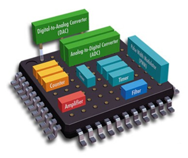
Fig. 1: Image of a Typical Programmable System on Chip (PSoC) Device
ARCHITECTURE OVERVIEW
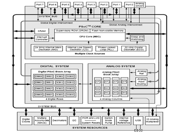
Fig. 2: Architectural Overview of PSoC System
The above figure depicts a high level architectural overview of PSoC. It consists of a fixed processor core, number of configurable blocks and interconnects. The main component is a digital block which is analogous to a configurable logic block in a FPGA.
A PSoC consists of four main elements
1. The PSoC core is common to all PSoC families. It consists of a 24MHz M8C CPU core, on-chip RAM and flash memories, multiple clock sources, a sleep-and-watchdog timer, and an interrupt controller.
2. The Digital System contains a number of digital blocks. Each digital block can be configured (and reconfigured) to perform one of several digital functions such as 32-bit timer, 16-bit PWM, UART and SPI.
3. The Analog System contains a number of analog blocks. Each analog block can be configured and reconfigured to perform one of several analog functions such as filters, amplifiers, tone generators, ADCs, and DACs.
4. System Resources include multiply-accumulates (MAC), decimators, I2C, a Switch Mode Pump (SMP), and a full speed (12Mbps) USB. These provide the chip with enhanced capability.
All the elements are connected through configurable interconnect which can be analog or digital in nature. This allows various blocks to be connected to each other. It also allows the blocks to drive or be driven away from available I/O pins. The configurable core of a PSoC is formed by the analog system, the digital system and the interconnect.
Analog System
Analog System
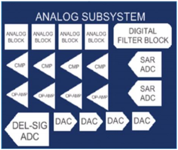
Fig. 3: Block Diagram of Analog System – A Component of PSoC System
The analog subsystem is a configurable system which consists of op-amps, filters, DAC, ADC. It also has low power comparators. There are two ADCs used. Delta-Sigma ADC has up to 20-bit resolution. A delta-sigma ADC first encodes an analog signal using high-frequency delta-sigma modulation. It then applies a digital filter to form a higher-resolution but lower sample-frequency digital output. It is used to transfer higher resolution digital signals to lower resolution. The ADC generates a pulse stream in which the frequency of pulses in the stream is proportional to the analog voltage input. The other type of ADC is Successive approximation (SAR) ADC which converts a continuous analog waveform into adiscrete digital representation using a binary search through all possible quantization levels. Along with this, it also has a digital filter block. The programmable analog blocks include mixer, trans-impedance amplifier and sample and hold.

Fig. 4: Block Diagram Showing Delta Sigma – ADC Details
BLOCK DIAGRAM OF DELTA-SIGMA ADC
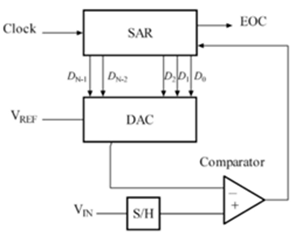
Fig. 5: Block Diagram of a SAR DAC
BLOCK DIAGRAM OF SAR ADC
The analog system has CapSense touch sensing enabled. CapSense is a capacitive sensing solution that has replaced around 3.5billion sensors with a capacitive touch interface. It provides flexibility so that the customer can make last minute changes. The CapSense controllers consume low power, provide robust noise immunity and have a wide voltage range. Capacitive sensing accepts the body capacitance as input.
Digital System
Digital System
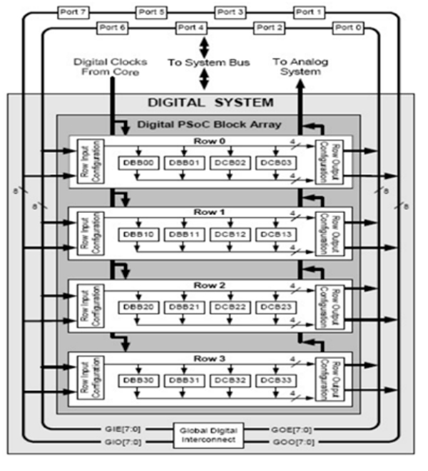
Fig. 6: Architectural Diagram of Digital System – A Component of PSoC System
DIGITAL SUBSYTEM
A digital system consists of digital blocks, global digital interconnect (GDI) and row digital interconnect (RDI). The RDI and GDI can route the inputs and outputs of any of the digital blocks between each other and to any of the on-chip I/O pins.The RDI connects the inputs and outputs of digital blocks to the GDI and the GDI connects the RDI to the on-chip I/O pins. Hence, RDI and GDI form the interconnect. This interconnect allows routing to and from the digital block. Various RAM based registers are programmed to configure the digital blocks and digital interconnect.
Dynamic reconfiguration of PSoC is established by storing specific configuration of these registers in the on-chip RAM. These can be loaded into the RAM as required.
1. Digital block
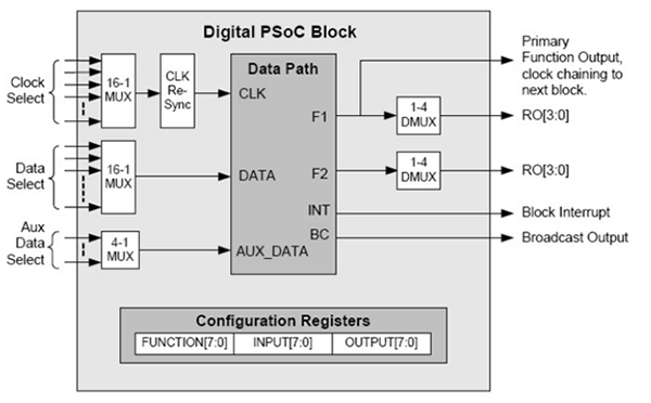
Fig. 7: Cross-Sectional Diagram of Digital Block of PSoC
A Digital Block consists of the data path, input multiplexers, output de-multiplexers, configuration registers, and chaining signal. A digital Block may be configured to perform any one of seven functions: timer, counter, pulse width modulator (PWM), pseudo random sequence (PRS), cyclic redundancy check (CRC), SPI, and a full duplex UART. The resolution provided is 8 bits. To obtain higher resolution, multiple blocks can be chained together.
It is the basic building block of the device.
2. Global Digital Interconnect
It includes four 8-bit buses which allow signals to pass to device pins from core or from device pins to core of the device. There are two buses for input and two for output. Among these, the input buses are called Global Input Odd (GIO) and Global Input Even (GIE) and the output buses are called Global Output Odd (GOO) and Global Output Even (GOE).
Odd busses connect to odd I/O ports such as ports 1, 3, 5, and 7 and even buses connect to even I/O ports like 0,2,4,6.
3. Row Digital Interconnect (RDI)
The RDI consists of four Row input nets and four row output nets. The function of Row input nets is to route signals from GDI to the input of the digital blocks. Each row input has a 4:1 MUX. The input to the MUX is given by four GDI lines. The outputs of these mux are Row Inputs. Any single Row Input net can connect to one of four possible GDI lines. As the inputs to the mux are unique to each mux, a complete Row Input has access to every global input line in a PSoC device.
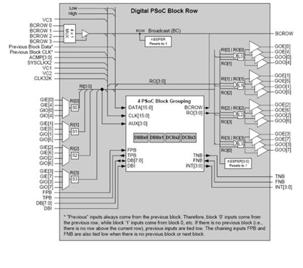
Fig. 8: Intricate Details of PSoC Digital Block
The four mux can be controlled by writing in to the Row Input register which is RAM based like other configuration registers. This means that it can be configured during start up, as well as during normal operation of the PSoC device thus allowing for dynamic reconfiguration of the input nets of the PSoC device.
The Row Output nets consist of 2-input Look Up Tables (LUT). The LUT allows the user to specify any of the 16 logic functions which can be applied to the two inputs. The figure below is an example of a Row Output net.
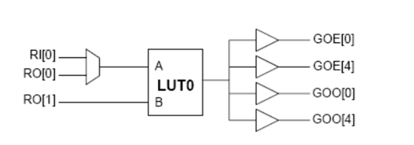
Fig. 9: An Example of Row Output Net in A PSoC
With the help of configurable tri-state buffers, the output of LUT can drive up to 4 GDI lines. The inputs, outputs, and logic functions of LUT are configured via RAM based registers. These can be loaded with settings stored in flash memory after power up or during normal operation of the device. This allows for initial configuration and dynamic reconfiguration of signal routing from the digital blocks to the output pins.
CPU Subsystem
CPU SUBSYSTEM
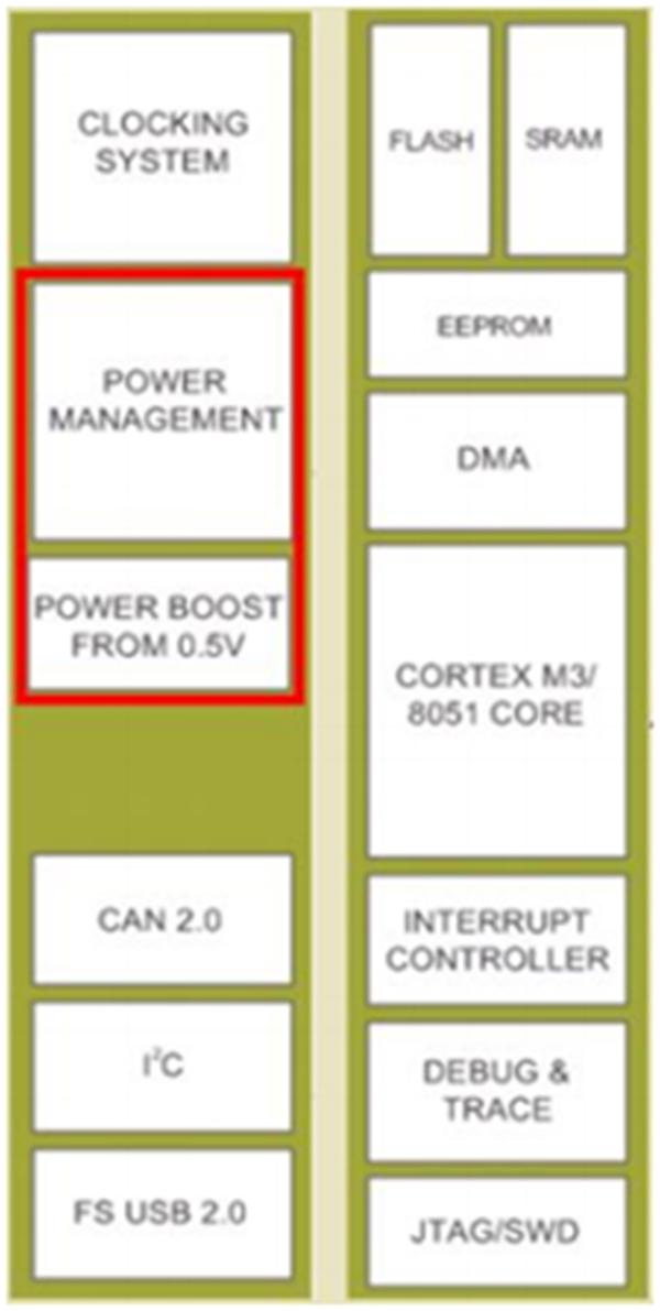
Fig. 10: Image Showing PSoC CPU Subsystem
The CPU subsystem of PSoC includes SRAM (Static Random Access Memory), EEPROM, flash memory and multiple core options. Other system resources include internal main and low-speed oscillator, connectivity to external crystal oscillator for precision, programmable clocking, sleep and watchdog timers and multiple clock sources that include a PLL.
THE PSoC SERIES
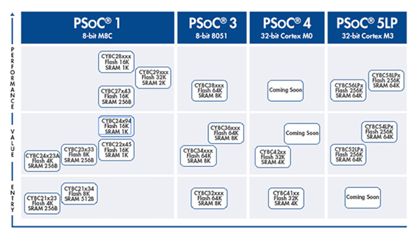
Fig. 11: An Overview of Different PSoC Series
There are five series of PSoC: PSoC1, PSoC3, PSoC4, PSoC5 and PSoC5L. The core of the CPU differs with each series. The PSoC1 has M8C CPU core, the PSoC3 has 8051 and the PSoC5 has ARM Cortex-M3.
PSoC1 is the world’s first Programmable embedded System-on-Chip. It has integrated configurable analog and digital peripheral functions, memory, and a microcontroller on a single chip. This device has changed the face of System-on-Chip. It has M8C core which is manufactured by Cypress. It is an 8 bit core which is the most cost effective solution in its category. It has performance of 24 MHz, 4 MIPS (million instructions per second). It has flash of 4 KB to 32 KB and SRAM of 256B to 2 KB.
The PSoC3 is powered by an 8-bit core which is the 8051. The CPU performance is up to 67MHz and 33MIPS which is a vast improvement from the previous series. The core is pipelined RISC core which improves the performance of the device. The PSoC3 architecture can run more than ten times faster than the standard 8051 architecture. PSoC 3 can handle dozens of data acquisition channels and analog inputs on every GPIO pin. It has a high-performance configurable digital system supporting a wide range of communication interfaces. It also has a 12 to 20 bit resolution delta-sigma modulation ADC. It has flash of size 8 KB to 64 KB and SRAM of size 2 KB to 8 KB.
The PSoC5 is powered by the ARM Cortex -M3 processor running up to 80 MHz at 100 DMIPS (Dhrystone Million Instructions per Second). The ARM Cortex- M3 uses THUMB instruction set architecture. It is ideal for migrating 8-bit and 16-bit applications in to 32 bit applications. This device can handle complex motor control algorithms requiring fast signal processing such as field oriented control (FOC), high-performance waveform generation for brushless motors and high-performance sensor applications. It has flash of32 KB to 256 KB and SRAM of 16 KB to 64 KB.
Programming and Advantages
PROGRAMMING OF PSoC
The software for PSoC1 is PSoC designer. Applications can be developed using a library of pre-characterized analog and digital peripherals in a drag-and-drop design environment. Then it can be customized with C or Assembly language. The design is completed in four easy steps:
1. Select user modules from a library of preconfigured analog and digital user modules.
2. Configure input and output drivers
3. Organize and connect modules using visual programmable interconnects
4. Program in C or Assembly with user module’s APIs and ISRs. Test with the tool’s debugger and in-circuit emulator.
The software for devices other than PSoC1 is PSoC creator. This has an additional option of Verilog entry. This software allows the user to : Create and share user-defined, custom peripherals using hierarchical schematic design and Verilog entry ,automatically place and route selected components and integrate simple glue logic normally residing in discrete muxes.
ADVANTAGES OF PSoC
Main advantages include flexibility, integration and programmable analog.
Flexibility
Programmable analog and digital blocks in PSoC provide the flexibility to adapt to changing requirements quickly and easily. Adding new features is relatively simple. Tuning and adjusting designs during debug/system bring-up is possible.
Integeration
Unmatched integration makes PSoC the fastest way to reduce the size, weight, and power requirements of any product. Dynamic reconfiguration allows reduction of testing costs by enabling dynamically configurable board self-tests. Additionally, one PSoC integrates as many as 100 peripheral functions.
Programmable Analog
Developing embedded systems with advanced analog sensing, monitoring, and control is simple with built-in programmable analog features. The PSoC solution includes a broad portfolio of preconfigured and characterized user components for CapSense capacitive touch sensing, voltagemonitoring, environmental sensing and fan/motor control.
APPLICATIONS
PSoC is used in variety of applications ranging from Adidas sneakers to the scroll wheel on the I-pod. It is used in Sonicare toothbrushes and TiVo set top box. This is due to its small size, flexibility, programmable analog system and low Time to market costs.
The Adidas shoe, adidas_1DLX uses PSoC mixed-signal array. It provides functionality like controlling user interface, monitoring heel strike pressure, controlling tensioning motor within the shoe’s heel. It adapts to the needs of every runner.
In the I-pod, One PSoC, using CapSense, controls the touch-sensitive scroll wheel on the Apple iPod click wheel.
Recently, it has been used in signal mixing applications and in fiber optic serial communication interface as well.
Filed Under: Articles


Questions related to this article?
👉Ask and discuss on Electro-Tech-Online.com and EDAboard.com forums.
Tell Us What You Think!!
You must be logged in to post a comment.