A FinFET is classified as a type of multi-gate Metal Oxide Semiconductor Field Effect Transistor (MOSFET). It was first developed at the University of Berkley, California by Chenming Hu and his colleagues. A multi-gate transistor incorporates more than one gate in to one single device. In FinFET, a thin silicon film wrapped over the conducting channel forms the body. The name has been derived from the fact that the structure, when viewed, looks like a set of fins. The thickness of the device determines the channel length of the device. The channel length of a MOSFET is said to be the distance between the source and drain junctions. It is a non-planar, double gate transistor which based either on the Bulk Silicon-On-Insulator (SOI) or on silicon wafers . It is based on the single gate transistor design.There are two types of FinFets:
1. Bulk FinFet
2. SOI FinFet
The ‘types’ of finfets are nothing but the ‘base’ onto which it is fabricated. This means that FinFets can be made either on SOI wafers or regular silicon wafers.
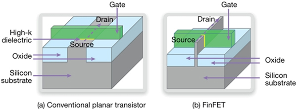
Fig. 1: Image Showing Constructional Difference Between Conventional Plane Transistor and FINFET
The gate of the FinFet is wrapped around (a wrap-around gate!) which reduces leakage current thereby increasing effectiveness.
NEED OF FINFET
Since the fabrication of MOSFET, the channel length of the device has been shrinking constantly so as to fabricate compact and fast devices. The following parameters related to MOSFET highlight the need for smaller, compact devices and explain why the MOSFET is not the suitable choice for the same. The shorter section of the gate electrode is known as the length and the longer section is called the width.
As the channel length of a MOSFET reduces, the short-channel effects increase. The short-channel effects are attributed to two physical phenomena:
a. The limitation imposed on electron drift characteristics in the channel
b. The modification of the threshold voltage due to the shortening channel length.
There are five different distinguishable short-channel effects :
A. Drain-induced barrier lowering
The two depletion layer merge as a result of depletion region surrounding the drain which extends to the source.. This leads to occurrence of punchtrough. Punchthrough can be reduced with the help of thinner oxides, larger substrate doping, shallower junctions, and also with longer channels.
B. Surface scattering
As the channel length becomes smaller, the longitudinal electric field component increases, and the surface mobility becomes field-dependent. The carrier transport in a MOSFET is confined within the narrow inversion layer. The surface scattering causes reduction of the mobility. The electrons find it difficult to move parallel to the interface. This is necessary so that the average surface mobility is about half as much as that of the bulk mobility. Surface scattering are the collisions suffered by the electrons which are accelerated toward the interface.
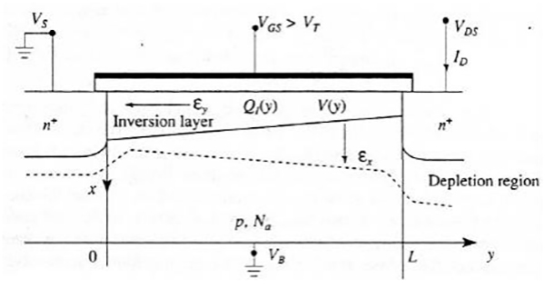
Fig. 2: Diagram Explaining Surface Scattering Phenomenon in FINFET Similar to MOSFET
C. Velocity saturation
Velocity saturation reduces transconductance in saturation mode. When a strong electric field is applied, carrier velocity reaches maximum value known as saturation velocity. When this occurs, the state of the transistor is known as velocity saturation. Velocity saturation is caused by the increased scattering rate of highly energetic electrons, primarily due to optical phonon emission.This effect increases the transit time of carriers through the channel.
D. Impact ionization
Thisusually occurs due to the high velocity of electrons in presence of high longitudinal fields that can generate electron-hole (e-h) pairs by impact ionization. Impact ionization occurs due to the impact on silicon and ionizing of the electron-hole pairs. It happens as follows: usually, most of the electrons are attracted by the drain, while the holes enter the substrate to form part of the parasitic substrate current. Also, the region between the source and the drain can act like the base of an N-P-N transistor. The source plays the role of the emitter and the drain that of the collector. If the holes are collected by the source, and the corresponding hole current creates a voltage drop in the substrate material of the order of .6V, the normally reversed-biased substrate-source P-N junction will conduct. Then electrons can be injected from the source to the substrate, similar to the injection of electrons from the emitter to the base. They can gain enough energy as they travel toward the drain to create new eh pairs. The situation can worsen if some electrons generated due to high fields escape the drain field to travel into the substrate, thereby affecting other devices on a chip.
E. Hot electron effect
Hot electron effect occurs when electrons or holes gain high kinetic energy due to the presence of high electric field within a semiconductor device. Hot electrons are more probable than hot holes since they have higher mobility to begin with. Hot carriers get injected or trapped in certain areas and cause undesirable device behaviour and degradation hence give rise to hot carrier Effects.
As the size of the devices is scaled down, the electric field of the channel increases. This leads to the high field region near the drain terminal occupying a large fraction of the channel length. This leads to the hot electron effect which in turn degrades the device parameters with time. This effect creates obstacles while scaling down the device.
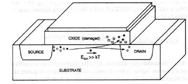
Fig. 3: Figure Showing Hot Electron Effect in FINFET
MOORE’S LAW
In 1965, Gordon Moore sketched out his prediction of the pace of silicon technology. Decades later, Moore’s Law remains true. Gordon Moore is the cofounder of Intel. He observed that the number of transistors per square inch on an integrated circuit (IC) doubled every year ever since the invention of an IC. This law is a crucial factor in the semiconductor industry in order to set targets and for long term planning.
Moore’s law is an observation or a projection and not a physical law. It describes the driving force of technological, economic, social and technological growth.
WORKING PRINCIPLE OF FINFET
The working principle of a FinFet is similar to that of a conventional MOSFET. The MOSFET can function in two modes: enhancement mode and deflection mode for both p-channel and n-channel MOSFETs.
The channel shows maximum conductance when there is no voltage on the gate terminal. As the voltage changes to positive or negative, the conductivity of the channel reduces.
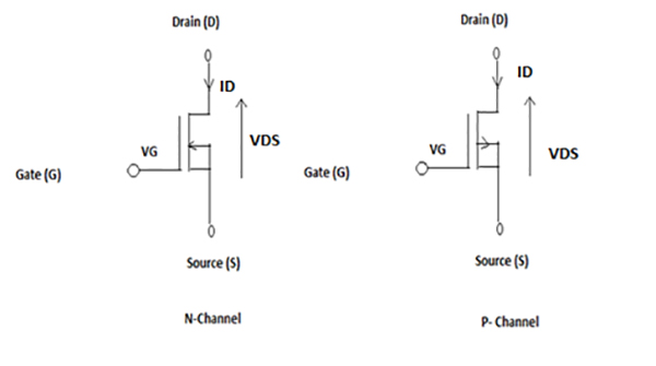
Fig. 4: Diagram Depicting Working Principle of FINFET Based on MOORE’S LAW
In enhancement mode of MOSFET, when there is no voltage on the gate terminal, it does not conduct. Unlike the depletion mode, in enhancement mode, the device conducts better when there is more voltage on the gate terminal.
The main aim of the MOSFET is to control the flow of voltage and current between the source and drain terminals. A high quality capacitor is formed by the gate terminal. The gate is composed of the silicon oxide layer, the p-body silicon and gate metallization and the p-body silicon. This capacitor is the most vital part. The semiconductor surface at the below oxide layer which is located between source and drain terminal. This is inverted from p-type to n-type by applying a positive or negative gate voltage respectively.
When a small amount of voltage is applied to this structure (the capacitor), keeping gate terminal positive with respect to source, a depletion region is formed. This depletion region is formed at the interface between the silicon and the SiO2.
The positive voltage applied attracts electrons from the source terminal, the drain terminal as well as the n+ source. This forms the electron reach channel. If we apply voltage between the source and drain terminals, current will flow between source and drain terminals. The concentration of electrons is controlled by the gate voltage (Vg).
The current equation can be expressed as follows
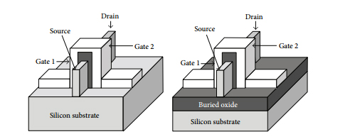
Fig. 5: Image Showing FIN etch Process
Where,
un = Mobility of the electrons
Cox = Capacitance of the oxide layer
W = Width of the gate area L = Length of the channel
VGS = Gate to Source voltage
VTH = Threshold voltage
VDS = Drain to Source voltage.
If we apply a negative voltage, a hole channel will be formed under the oxide layer. Now, the controlling of source to gate voltage is responsible for the conduction of current between source and the drain. If the gate voltage exceeds a given value, only then does the conduction begins.
CONSTRUCTION OF FINFET:
The two types of FinFets have different construction. The basic layout and mode of operation are similar to that of a conventional MOSFET. The only difference is the three dimensional bar atop the silicon substrate- the fin.
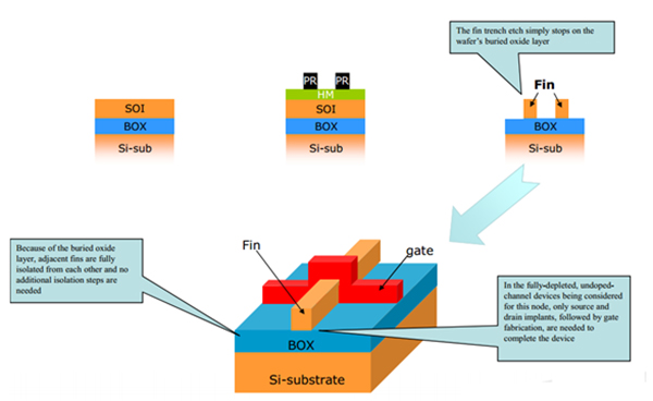
Fig. 6: Figure Showing Construction of FD-SOI FINFET
![]()
Fig. 7: Image Showing Construction of Silicon-Based Bulk FINFET
silicon based FinFet
The important characteristics of this FinFet is that the conducting channel is wrapped by a thin Si fin. This forms the body of the device. The fins are the 3D channel between the source and the drain terminals.they are built on top if silicon (Si) substrate. The gate terminal is wrapped around the channel. This allows formation of several gate electrodes so as to reduce leakage current and enhance the drive current.
1. Substrate:
The base of a FinFET is a lightly p-doped substrate with a hard mask on top. It also has a patterned resist layer.
2. Fin etch:
The fins are formed in a highly anisotropic etch process.Absence of a stop layer forces the etch process to be time based. This layer is present in the SOI models.
![]()
Fig. 8: Image Showing Deposition of n+-doped Poly Silicon Layer in FINFET Construction
3. Oxide deposition: An oxide deposition with a high aspect ratio filling behaviour is needed so as to separate the fins from one another.
4. Planarization: The oxide is planarized by chemical mechanical polishing. In this, the hard mask acts as a stop layer.
5. Recess etch: this process is needed so as to recess the oxide film to form a lateral isolation of the fins.
6. Gate oxide: On top of the fins the gate oxide is deposited via thermal oxidation to isolate the channel from the gate electrode. Since the fins are still connected underneath the oxide, a high-dose angled implant at the base of the fin creates a dopant junction and completes the isolation.
7. Deposition of the gate: Finally a highly n+-doped poly silicon layer is deposited on top of the fins. This leads to wrapping of three gates around the channel: one on each side of the fin, and a third gate above. The third gate is wrapped depending on the thickness of the gate oxide which is on top.
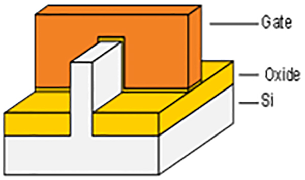
Fig. 9: 2-D View of Layers of FINFET
The influence of the top gate can also be inhibited by the deposition of a nitride layer on top of the channel.
Due to the presence of an oxide layer on an SOI wafer, the channels are isolated from each other anyway. Along with this, the etch process of the fins is simplified. This is done because the process can be easily stopped on the oxide.

Fig. 10: 3-D View of FINFET Structure
APPLICATIONS OF FINFET
World leader in smartphones, Samsung Electronics has incorporated FinFet in its 14nm processors (Exynos7 Octra). This processor is used in the latest Samsung smartphone, the Samsung Galaxy S6. They teamed up with Globalfoundries for this project.
Along with Samsung, Apple, Intel and TSMC are set to ship the 14nm technology by 2016. This technology will benefit all smartphones as it will speed up the phone. This technology has surpased the previous technologies by overcoming scaling and performance limitations faced while using the 20nm technology.
FUTURE SCOPE
Future scope of FinFet include further scaling down to 10nm. The optimization of the transistor fin will play a crucial role in this development. Further research is being conducted to scale down the FinFet so as to improve efficiency. It is worth mentioning that 14nm size is equivalent to the size of a virus. We have definitely come a long way in terms of scaling down a transistor. So the next time you complain about the price of the iphone or the new Samsung smartphone, remember that the technology it uses will not be found in most other phones!
Filed Under: Articles


Questions related to this article?
👉Ask and discuss on Electro-Tech-Online.com and EDAboard.com forums.
Tell Us What You Think!!
You must be logged in to post a comment.