While dealing with controllers we are dealing with digital signals but real world is analog. In real world all natural quantities like temperature, pressure, light intensity etc. are analog. If we have to deal with such quantities using embedded systems, we have to convert these analog quantities which can be understood and proceed by digital signal. Devices used for this purpose is known as ADC. Special ICs such as ADC0804, ADC0808, ADC0809, Serial ADC MAX1112 etc. are handy for this. Nowadays, many controllers are having inbuilt ADC. LPC2148 of ARM7 family is one of the widely used controller and it also has multichannel ADC inbuilt. In this article, we will understand how to use inbuilt ADC of LPC2148.
 ADCs act as a bridge between the analog real world and the digital world of controllers. ADC converts analog voltage into a digital number, which can be understood and proceed by the controller. Let us understand this with an example.
LPC 2148 operates on a 3.3V supply. Suppose we use 10 bit ADC, 3.3V correspondences to 2^10=1023. Half of 3.3V= 1.65V can be represented by 512, 0V as digital value 0, and so on.
Before proceeding further, let us first understand a few basic concepts related to ADC.
1. Resolution:
Analog voltage will be converted into a digital number. The number of bits required to store the digital number, let say n bits, is known as resolution. If a digital number is represented with n bits, the maximum value is 2n. So for 10 bit ADC resolution is 10 bit, and the maximum value is 210=1023.
2. Step size
Minimum voltage, which can be distinguished by the controller, is known as the step size.
Step size= Maximum Voltage/ 2n where n= resolution
For LPC 2148, Maximum voltage=3.3V and n=10
So step size=3.3/1023= 0.0032258064 V = 3.23 mv (Approx.)
The voltage between 0 and 3.23 mV will be identified as the same for the controller. This identifies the accuracy of ADC.
3. Conversion time
Converting analog voltage into digital will not be done immediately. It will take a few mili-seconds. The higher the resolution, the higher is the conversion time.
So now, let us start with the ADC of LPC 2148. First, let us have a quick look at the features of it.
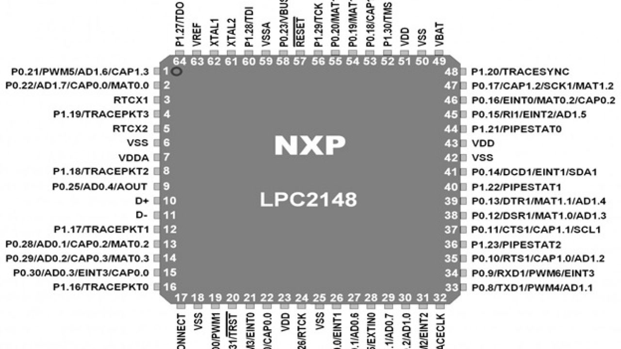
> LPC 2148 has two inbuilt ADC modules known as ADC0 and ADC1.
> Maximum resolution of ADC is 10 bit. It is configurable by programming.
> ADC0 has 6 channels
> ADC1 has 8 channels
> Both ADC supports a maximum clock frequency of 4.5 MHz (Operating frequency decides the conversion time)
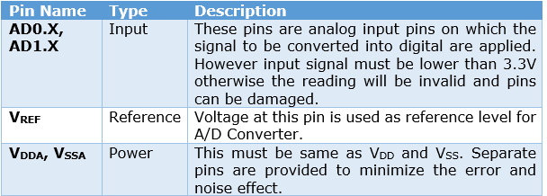
Pins required for ADC are as follows.
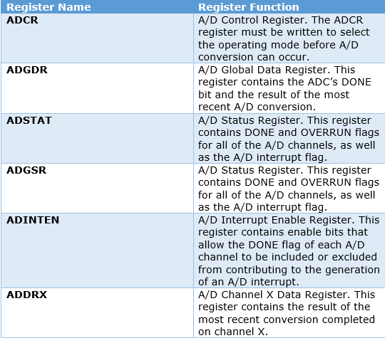
There are various registers associated with ADC0 and ADC1. Commonly user registers are ADC Control Registers (AD0CR & AD1CR) and ADCGR- ADC Global data register.
Let us understand all registers one by one.
The most important register for ADC is ADCR. Let us see the functions of each bit of this register.


Another important register is AD0GR and AD1GR. Bits of this register are as follows.

The result of the conversion is stored in the A/D Data register, which has the following structure.

Steps for programming:
1. Configure input pin as an analog input pin for ADC
2. Select channel of ADC
3. Start conversion
4. Wait till conversion is done
5. Read data of ADC Conversion output
6. Convert number into separate digits like 512 as separate 5,1 and 2
7. Display digits on LCD
8. Repeat the above steps
Project Source Code
###
//Program to Interface ADC with LPC2148#include/* LPC21xx definitions */ #include "lcd4bit.h"void init_adc(){PINSEL1 |= 0X01000000;ADCR = 0X00200602;}void delay(int n) /* generates one milisecond delay */{int i,j;for (i=1; i<=n; i++)for(j=0; j<=10000; j++);}int read_adc(void){int val;ADCR |= 0x01000000; /* Start A/D Conversion */do {val = ADDR; /* Read A/D Data Register */} while (!(val & 0x80000000)); /* Wait for end of A/D Conversion */ADCR &= ~0x01000000; /* Stop A/D Conversion */val >>=6;val= val & 0x3FF;return(val);}int main(void){int dat,i=0;char buf[5];init_adc();init_lcd();lcd_command(0x01);lcd_command(0x80);printlcd("ADC Interfacing");lcd_command(0xC0);printlcd("with LPC2148");delay(2000);lcd_command(0x01);lcd_command(0x80);printlcd("Developed By:");lcd_command(0xC0);printlcd("Dishant Shah");delay(2000);lcd_command(0x01);lcd_command(0x80);printlcd(" EMERTECH ELE. ");lcd_command(0xC0);printlcd("SYSTEMS,Vadodara");delay(3000);lcd_command(0x01);lcd_command(0x80);printlcd("Digital Value");lcd_command(0xC0);while(1){Delay(1000000);lcd_command(0xC0);dat = read_adc();i=0;while(dat>0){buf[i]=dat%10;dat=dat/10;i++;}while(--i >= 0){lcd_data(buf[i]+'0');}delay(10);}}
###
Project Source Code
###
//Program to Interface LCD with LPC2148#include#include "lcd4bit.h"void Delay(unsigned long b){while (--b!=0);}void write_command(int cmd) {IO1CLR |= 0x00f00000; /* Clear D4-D7 */IO1CLR |= 0x00040000; /* Read/Write = 0 */IO1CLR |= 0X00020000; /* Register Select = 0,Command */IO1SET |= 0x00f00000 & cmd; /* Set D4-D7 */IO1SET |= 0X00080000; /* Enable = 1 */Delay(30000);IO1CLR |= 0x00080000; /* set E to low */}void write_data(int dat) {IO1CLR |= 0x00f00000; /* Clear D4-D7 */IO1CLR |= 0x00040000; /* Read/Write = 0 */IO1SET |= 0X00020000; /* Register Select = 1,Data */IO1SET |= 0x00f00000 & dat; /* Set D4-D7 */IO1SET |= 0X00080000; /* Enable = 1 */Delay(30000); //delay ~2msIO1CLR |= 0x00080000; /* Set E to low */}void lcd_data(char dat){write_data(dat << 16);write_data(dat << 20);}void lcd_command(char cmd){write_command(cmd << 16);write_command(cmd << 20);}void printlcd(char *CPtr){while(*CPtr != '') {lcd_data(*CPtr);CPtr++;Delay(20000);}}void init_lcd(void) {IO1DIR |= 0x00FE0000;Delay(200000) ;write_command(0x30 << 16);Delay(100000);write_command(0x30 << 16);Delay(100000);write_command(0x30 << 16);Delay(100000);write_command(0x20 << 16);lcd_command(0x01); /* clear display */lcd_command(0x06); /* auto address inc */lcd_command(0x0c); /* cursor off */lcd_command(0x80); /* first location */}
###
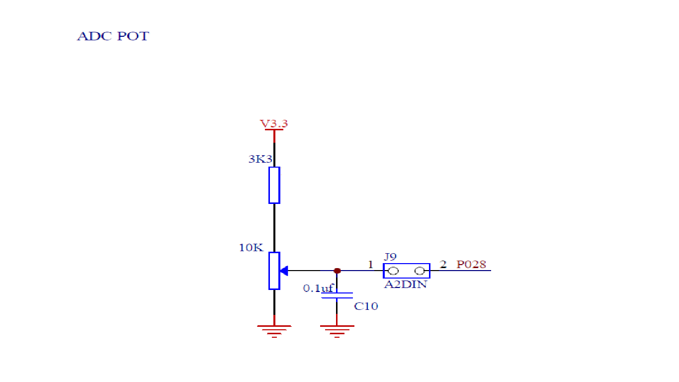
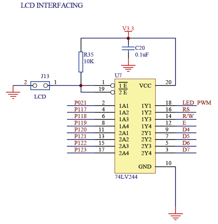
Circuit Diagrams
Project Video
Filed Under: ARM.
Filed Under: ARM.

Questions related to this article?
👉Ask and discuss on EDAboard.com and Electro-Tech-Online.com forums.
Tell Us What You Think!!
You must be logged in to post a comment.