It is necessary to understand basic I/O operations of PIC18F4550 before dealing with its complexities. This article presents a way to take simple output from a PIC microcontroller. This learning would also help in interfacing of external devices with the controller. Here the output from the microcontroller is taken on a set of LEDs which are made to blink in an alternate fashion.
PIC18F4550 has a total of 35 I/O (input-output) pins which are distributed among 5 Ports. The following table shows the names and numbers of I/O pins of these 5 ports:
|
Port Name
|
Number of Pins
|
Pins
|
|
PORTA
|
7
|
RA0-RA6
|
|
PORTB
|
8
|
RB0-RB7
|
|
PORTC
|
7
|
RC0-RC2, RC4-RC7
|
|
PORTD
|
8
|
RD0-RD7
|
|
PORTE
|
4
|
RE0-RE3
|
Fig. 2: I/O pins name and numbers of various ports in PIC
As opposed to a basic 8051 microcontroller like AT89C51 which has most of the port pins serving single function, the port pins of a PIC microcontroller are multiplexed to serve more than one purpose.
The 35 I/O pins of PIC18F4550 are also multiplexed with one or more alternative functions of controller’s various peripherals. Each Port of a PIC microcontroller corresponds to three 8-bit registers which should be configured to use the Port for general I/O purpose. These registers are:
1. TRISx: This is a data direction register which sets the direction of each port pin as input or output.
2. PORTx: This register stores the input level of pins (High or Low). When a pin configured as input, the input signal from external source is read from PORTx register.
3. LATx: This is output latch register. The data which has to be sent to external hardware as output is stored in LATx register.
Port Description:
PORTA:
PortA has 7 pins which can be used as both input as well as output pin. The 7th bit is missing from all the three registers. The input and output given to this port are of 8-bit but the 8th bit is internally masked.
|
|
Bit 7
|
Bit 6
|
Bit 5
|
Bit 4
|
Bit 3
|
Bit 2
|
Bit 1
|
Bit 0
|
|
TRISA
|
–
|
TRISA6
|
TRISA5
|
TRISA4
|
TRISA3
|
TRISA2
|
TRISA1
|
TRISA0
|
|
PORTA
|
–
|
RA6
|
RA5
|
RA4
|
RA3
|
RA2
|
RA1
|
RA0
|
|
LATA
|
–
|
LATA6
|
LATA5
|
LATA4
|
LATA3
|
LATA2
|
LATA1
|
LATA0
|
Fig. 3: PortA Configuration in PIC
PORTB:
PortB has 8 pins which can all be used for both input and output operation.
|
|
Bit 7
|
Bit 6
|
Bit 5
|
Bit 4
|
Bit 3
|
Bit 2
|
Bit 1
|
Bit 0
|
|
TRISB
|
TRISB7
|
TRISB6
|
TRISB5
|
TRISB4
|
TRISB3
|
TRISB2
|
TRISB1
|
TRISB0
|
|
PORTB
|
RB7
|
RB6
|
RB5
|
RB4
|
RB3
|
RB2
|
RB1
|
RB0
|
|
LATB
|
LATB7
|
LATB6
|
LATB5
|
LATB4
|
LATB3
|
LATB2
|
LATB1
|
LATB0
|
Fig. 4: PortB Configuration in PIC
PORTC:
PortC has 7 I/O pins. In PortC, Bit 3 is missing in hardware and Pins 4 & 5 can only be used as input pins. There are no 4th & 5th latch bits in LATC register, so these bits are internally masked during 8-bit write operation on PortC.
|
|
Bit 7
|
Bit 6
|
Bit 5
|
Bit 4
|
Bit 3
|
Bit 2
|
Bit 1
|
Bit 0
|
|
TRISC
|
TRISC7
|
TRISC6
|
–
|
–
|
–
|
TRISC2
|
TRISC1
|
TRISC0
|
|
PORTC
|
RC7
|
RC6
|
RC5
|
RC4
|
–
|
RC2
|
RC1
|
RC0
|
|
LATC
|
LATC7
|
LATC6
|
–
|
–
|
–
|
LATC2
|
LATC1
|
LATC0
|
Fig. 5: PortC Configuration in PIC
PORTD:
PortD has 8 pins which can all be used for both input and output operation.
|
|
Bit 7
|
Bit 6
|
Bit 5
|
Bit 4
|
Bit 3
|
Bit 2
|
Bit 1
|
Bit 0
|
|
TRISD
|
TRISD7
|
TRISD6
|
TRISD5
|
TRISD4
|
TRISD3
|
TRISD2
|
TRISD1
|
TRISD0
|
|
PORTD
|
RD7
|
RD6
|
RD5
|
RD4
|
RD3
|
RD2
|
RD1
|
RD0
|
|
LATD
|
LATD7
|
LATD6
|
LATD5
|
LATD4
|
LATD3
|
LATD2
|
LATD1
|
LATD0
|
Fig. 6: PortD Configuration in PIC
PORTE:
PortE has 4 I/O pins. Pin3 can be used as input pin only. RDPU bit is used to enable/disable internal pull-ups of PortD.
|
|
Bit 7
|
Bit 6
|
Bit 5
|
Bit 4
|
Bit 3
|
Bit 2
|
Bit 1
|
Bit 0
|
|
TRISE
|
–
|
–
|
–
|
–
|
–
|
TRISE2
|
TRISE1
|
TRISE0
|
|
PORTE
|
RPDU
|
–
|
–
|
–
|
RE3
|
RE2
|
RE1
|
RE0
|
|
LATE
|
–
|
–
|
–
|
–
|
–
|
LATE2
|
LATE1
|
LATE0
|
Fig. 7: PortE Configuration in PIC
I/O configuration:
The TRISx register is configured to set a pin as input or output. The High value (1) sets a pin as input pin and Low value (0) sets a pin as output. An easy way to remember this is to consider the resemblance of 1 with the letter I (for input) and 0 with the letter O (for output).
For example suppose a switch is connected at RB0 and an LED is connected to RB7 of PortB. Now the pins 0 & 7 have to be configured as input and output respectively. So the bit TRISB0 is set to 1 to configure RB0 as input pin & bit TRISB7 is set to 0 to configure RB7 as output pin.
|
TRISB
|
TRISB7
|
TRISB6
|
TRISB5
|
TRISB4
|
TRISB3
|
TRISB2
|
TRISB1
|
TRISB0
|
|
Value
|
0
|
…
|
…
|
…
|
…
|
…
|
…
|
1
|
Fig. 8: TRISB0 set as 1 to configure RB0 as input to interface LED in PIC
The unused bits are set to 0.
|
TRISB
|
TRISB7
|
TRISB6
|
TRISB5
|
TRISB4
|
TRISB3
|
TRISB2
|
TRISB1
|
TRISB0
|
|
Value
|
0
|
0
|
0
|
0
|
0
|
0
|
0
|
1
|
So the overall value of TRISB register becomes:

Fig. 9: Overall value of TRISB register to Interface LED with PIC
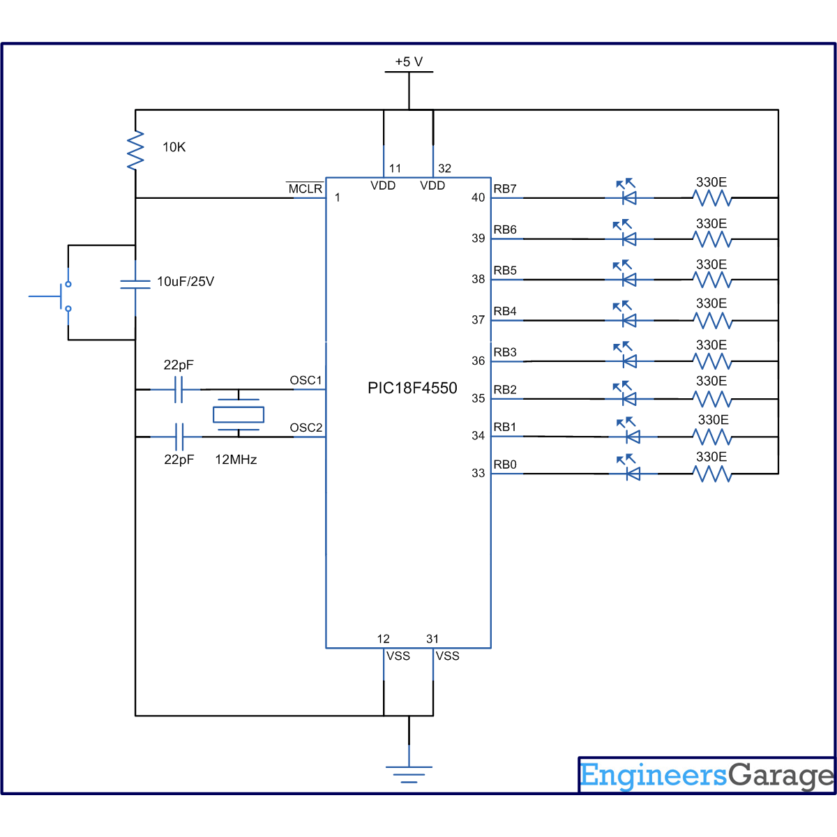
Using this knowledge, the objective of this article can be achieved which is to glow a set of LEDs in alternate blinking fashion. The LEDs here are connected to PORTB pins as shown in the circuit diagram.
Programming steps:
1. Configure the TRISB register to make PortB as output port.
2. Set all the bits of LATB register High (1) to glow all LEDs.
3. Provide some delay.
4. Set all the bits of LATB register Low (0) to turn off the LEDs.
5. Provide some delay.
6. Repeat the process from step 2.
Project Source Code
###
/******************Chip config*******************PLLDIV = 5CPUDIV = OSC1 / 2USBDIV = 2FOSC = HIGH_SPEED HSFCMEN = OFFIESO = OFFPWRT = OFFBOR = OFFBORV = 3VREGEN = OFFWDT = OFFWDTPS = 1:32768CCP2MX = ONPBADEN = OFFLPT1OSC = OFFMCLRE = OFFSTVREN = ONLVP = OFFICPRT = OFFXINST = OFFDEBUG = OFFCP0 = OFF, CP1 = OFF, CP2 = OFF, CP3 = OFFCPB = OFFCPD = OFFWRT0 = OFF, WRT1 = OFF, WRT2 = OFF, WRT3 = OFFWRTC = OFFWRTB = OFFWRTD = OFFEBTR0 = OFF, EBTR1 = OFF, EBTR2 = OFF, EBTR3 = OFFEBTRB = OFF******************Chip config*******************/#include <p18cxxx.h>void delay_ms ( int delay );void delay_ms ( int delay ){int ms, i;for ( ms = 0; ms < delay; ms ++ )for ( i = 0; i < 5; i ++ );}void main(){TRISB = 0x00; // Set PORTB as output PORTLATB = 0xFF; // Set PORTB high initially (All LEDs on)while ( 1 ){LATB = ~LATB; // Toggle the value of PORTBdelay_ms ( 1000 ); // Delay of 1 sec}}###
Circuit Diagrams
Project Components
Project Video
Filed Under: PIC Microcontroller.
Filed Under: PIC Microcontroller.

Questions related to this article?
👉Ask and discuss on EDAboard.com and Electro-Tech-Online.com forums.
Tell Us What You Think!!
You must be logged in to post a comment.