A transistor is a device that controls the current flowing into the channel of a low-power electrical signal application. They are classified in two ways:
1. Bipolar junction transistors (BJTs). A current-controlled device since a small amount of current is used to control its flow into a channel.
2. Field-effect transistors (FETs). A voltage-controlled device because a small voltage is used to control the current that flows into a channel.
This article focuses on the various types of FETs and includes a comparison chart.
Junction field-effect transistor (JFET)
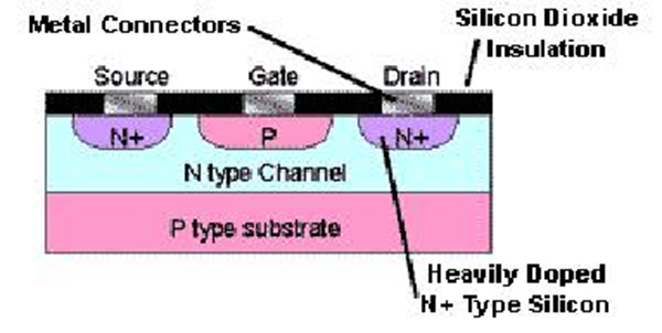
In a JFET, a thin layer of resistive N- or P-type semiconductor material forms a channel. Typically, N- or P-type silicon is used, which allows most carriers to flow through with two ohmic electrical connections (called the “drain” and “source”) formed at either end of the channel. A third ohmic contact (the “gate”) is also formed.

The various layers of a JFET.
A voltage that’s applied to the gate controls the current flowing through the channel. When a drain-to-source voltage causes the drain current to flow into the resistive channel, the current is equally distributed to all parts.
However, because of its resistive nature, a small gradient is formed that reduces in magnitude as the flow moves from the drain to the source terminal. This results in a PN junction with a larger reverse bias at the drain terminal and a smaller reverse bias at the source terminal.
This bias forms a depletion layer within the channel. Its width increases with the bias.
FETs are classified as either:
1. N-channel JFET – dopant impurities that make a negative flow current in the form of electrons.
2. P-channel JFET – acceptor impurities that make a positive flow current in the form of holes.
N-channel JFETs are preferred over P-channel JFETs because electrons offer more conduction than holes.
Applications
- As a low-noise, high-impedance amplifier.
- As a buffer amplifier with high-input impedance and low-output impedance.
- As RF amplifiers in the communication unit’s receiver section (because a JFET is ideal in low-current signal operations).
- As analog multiplexers, which can be made by using JFETs.
Metal oxide semiconductor field-effect transistor (MOSFET)
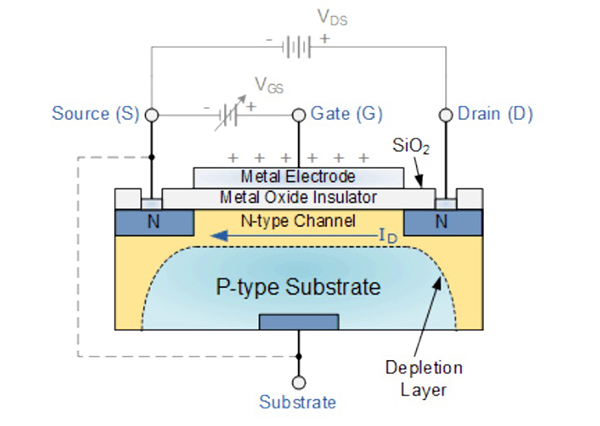
A MOSFET is a three-terminal device with a gate electrode that’s a metal oxide semiconductor, electrically insulated from the current-carrying channel by a thin layer of silicon dioxide (called “glass”).
The isolation of the gate electrode makes the input resistance extremely high — in the order of a few mega-ohms. As a result, MOSFETs are easily damaged by a high accumulation of static charges.
The construction of a MOSFET.
The gate terminal uses an electric field to alter the flow of carriers in the channel. The gate electrode is placed on top of thin insulating material with a pair of N-regions below the drain and source terminals.
As mentioned, a JFET is biased and will typically reverse bias the PN junction, but no such conditions exist in a MOSFET. However, they can be biased by a positive or negative polarity. Aside from classifying a MOSFET as an N- and P-type, there are two additional types available.
1. Depletion type MOSFET – the transistor can switch ON without applying the gate bias, which is equivalent to a “normally closed switch.”
2. Enhancement Type MOSFET – the transistor can switch ON with the gate bias application, which is equivalent to a “normally open switch.”
Applications:
- Millions of MOSFETs are integrated with digital ICs, such as microprocessors and memory devices, for implementing logic gates and data storage.
- Used as a switched-mode power supply and variable frequency drives.
- Used as analog signal and power amplifiers in RF amplifiers up to UHF.
- Used as oscillators and mixers to convert the frequencies in radio systems.
Heterojunction field-effect transistor (HFET)
Field-effect transistors used for high-speed applications — such as mobile phones — are either high-electron-mobility transistors (HEMT) or heterojunction field-effect transistors (HFET).
These transistors incorporate materials with different bandgaps. The channel is made of two different materials (in contrast to the doping used in MOSFETs), making it ideal for high-speed applications.

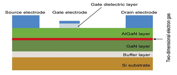
Construction of an HFET used for high-speed applications.
A variety of material combinations can be used depending on the demands of the application. Gallium nitride (GaN) and aluminum gallium nitride (AlGaAs) are now the most common materials. Once thought to have high-power performance, indium has been replaced by GaN, which has high-frequency responses.
Unlike other FETs, HFETs operate differently. For effective conduction, semiconductors are doped with materials that provide a sufficient amount of mobile electrons and holes. However, these electrons lose all their energy during collisions and do not contribute much to the conduction. This is not the case with HFETs.
Since HFETs use two materials — AlGaN (with a highly doped wide bandgap) and GaN (a non-doped narrow bandgap) — high electron mobility is achieved when the electrons from a thin N-type layer of AlGaN fall freely into GaN-making a depleted AlGaN layer.
These “falling” electrons then move freely in Gan’s conduction band without escaping or colliding with impurities. This is because GaN is not doped and has a higher affinity. The electrons form a very thin conducting layer with higher concentration, giving the channel low resistivity and high electron mobility. This layer is called 2D electron gas.
HFETs are either:
1. pHEMT (pseudomorphic HEMT) – uses heterojunction materials with different lattice constants.
2. mHEMT (metamorphic HEMT) – has a buffer layer between the two heterojunction materials.
Applications:
- As low-noise, small-signal amplifiers, power amplifiers, oscillators, and mixers.
- As RF design applications when incorporated into monolithic-integrated circuits.
- As electronic warfare systems, such as radar and radio astronomy.
Comparing JFETs, MOSFETs, and HFETs
|
JFET |
MOSFET |
HFET |
||
|
Material used |
Mostly silicon |
Mostly silicon |
III-V and Si, SiGe |
|
|
Input impedance |
High |
Very high |
High |
|
|
Gate terminal |
PN junction |
Insulated gate |
Schottky gate |
|
|
Gate current |
Leakage current |
No gate current |
Small gate current |
|
|
Channel |
Depletion channel |
Inversion channel |
Accumulation channel |
|
|
Types |
N- and P-channels | N- and P-channels |
Mostly N-type HFET |
|
|
Channel JFET |
Channel MOSFET |
|||
|
Substrate node |
Biased |
Biased |
Not biased (connected to the ground) |
|
|
No such mode exists |
||||
| Mode of operation | Depletion mode | Depletion and enhancement modes | ||
|
Applications |
Analog multiplexers, |
SMPS, microprocessors |
Low-noise amplifiers, RF design |
|
| Systems | RF amplifiers | Memory devices | Electronic warfare | |
|
|
|
|||
|
|
||||
|
|
|
|||
|
|
||||
|
|
|
|||
|
|
||||
Filed Under: Articles, Tech Articles


Questions related to this article?
👉Ask and discuss on EDAboard.com and Electro-Tech-Online.com forums.
Tell Us What You Think!!
You must be logged in to post a comment.