In the previous projects, adjustable power supply circuits were designed. Sometimes, the voltage to drive a specific circuit is already known and power supply circuit to output a constant voltage needs to be designed. In this project, a constant 12V power supply circuit is designed with an aim to power LED circuits. The circuit needs to be designed in a way that it should be void of any fluctuations or ripples. The circuit will input supply from main AC supplies and will convert it to a ripple free 12V DC supply. The circuit will be able to draw a maximum current of 1A.
In LED circuits, the excess flow of current through LEDs greater than their forward current rating can increase their temperature beyond limit damaging them permanently or temporarily. Therefore, a constant voltage supply is importantly required in such cases. A single LED or a combination of LEDs that requires net 12V input can be connected to the output of the circuit designed in this project.
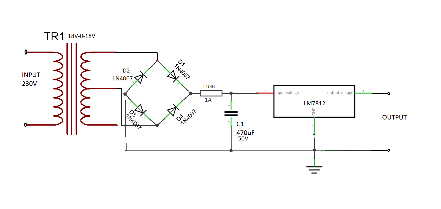
The power circuit designed in this project uses 7812 voltage regulator IC and uses conventional steps of power circuit design like stepping down AC voltage, converting AC voltage to DC voltage, and Smoothing DC voltage for getting direct input from the AC mains.
Components Required –

Fig. 1: List of Components required for Constant 12V Power Supply for LED Circuits
Block Diagram –

Fig. 2: Block Diagram of Constant 12V Power Supply for LED Circuits
Circuit Connections –
The circuit is assembled in stages with each stage serving a specific purpose. For stepping down the 230 V AC, an 18 V – 0 – 18 V transformer is taken. The secondary coil of the transformer is connected with a full-bridge rectifier. The full bridge rectifier is built by connecting four 1N4007 diodes to each other designated as D1, D2, D3 and D4 in the schematics. The cathode of D1 and anode of D2 is connected to one of the secondary coil and cathode of D4 and anode of D3 is connected to the centre tape of the secondary coil. The cathodes of D2 and D3 are connected from which one terminal is taken out from output of rectifier and anodes of D1 and D4 are connected from which other terminal is taken out the output from full-wave rectifier. A wire is drawn from the center tape of the transformer which serves as the ground for the positive and negative DC outputs.
A fuse of 1A is connected in series to the output of full-wave rectifier for protection from the AC supplies. A capacitor of 470 uF (shown as C1 in schematics) is connected between the output terminals of the full-wave rectifier for smoothing purpose. For voltage regulation, LM-7812 IC is connected in parallel to the smoothing capacitor. The output is drawn from the voltage output terminal of the 7812 IC.
How the circuit works –
The power circuit operates in well-defined stages with each stage serving a specific purpose. The circuit operates in the following stages –
1. AC to AC Conversion
2. AC to DC Conversion – Full Wave Rectification
3. Smoothing
4. Voltage Regulation
AC to AC conversion
The voltage of Main Supplies (Electricity fed by the intermediate transformer after stepping down line voltage from generating station) is approximately 220-230V AC which further needs to be stepped down to 12V level. To reduce the 220V AC to 12V AC, a step-down transformer with center taping is used. The use of center tap transformer allows to generate both positive and negative voltage at the input, however, only positive voltage will be drawn from the transformer. The circuit takes some drop in the output voltage due to resistive loss. Therefore a transformer of high voltage rating greater than the required 12 V needs to be taken. The transformer should provide 1A current at the output. The most suitable step-down transformer that meets the mentioned voltage and current requirements is 18V-0-18V/2A. This transformer step downs the main line voltage to +/-18V AC, as shown in the below image.

Fig. 3: Circuit Diagram of 18-0-18V Transformer
AC to DC conversion – Full Wave Rectification
The stepped down AC voltage needs to be converted to DC voltage through rectification. The rectification is the process of converting AC voltage to DC voltage. There are two ways to convert an AC signal to the DC one. One is half wave rectification and another is full wave rectification. In this circuit, a full-wave bridge rectifier is used for converting the 36V AC to 36V DC. The full wave rectification is more efficient than half wave rectification since it provides complete use of both the negative and positive sides of AC signal. In full wave bridge rectifier configuration, four diodes are connected in such a way that current flows through them in only one direction resulting in a DC signal at the output. During full wave rectification, at a time two diodes become forward biased and another two diodes get reverse biased.

Fig. 4: Circuit Diagram od Full Wave Rectifier
During the positive half cycle of the supply, diodes D2 and D4 conduct in series while diodes D1 and D3 are reverse biased and the current flows through the output terminal passing through D2, output terminal and the D4. During the negative half cycle of the supply, diodes D1 and D3 conduct in series, but diodes D1 and D2 are reverse biased and the current flows through D3, output terminal and the D1. The direction of current both ways through the output terminal in both conditions remain the same.

Fig. 5: Circuit Diagram showing positive cycle of Full Wave Rectifier

Fig. 6: Circuit Diagram showing negative cycle of Full Wave Rectifier
The 1N4007 diodes are chosen to build the full wave rectifier because they have the maximum (average) forward current rating of 1A and in reverse biased condition, they can sustain peak inverse voltage up to 1000V. That is why 1N4007 diodes are used in this project for full wave rectification.
Smoothing
Smoothing is the process of smoothing or filtering the DC signal by using a capacitor. The output of the full-wave rectifier is not a steady DC voltage. The output of the rectifier has double the frequency of main supplies but contains ripples. Therefore, it needs to be smoothed by connecting a capacitor in parallel to the output of full wave rectifier. The capacitor charges and discharges during a cycle giving a steady DC voltage as an output. So, a capacitor (shown as C1 in schematics) of high value is connected to the output of rectifier circuit. As the DC which is to be rectified by the rectifier circuit has many AC spikes and unwanted ripples, so to reduce these spikes capacitor is used. This capacitor acts as a filtering capacitor which bypasses all the AC through it to ground. At the output, the mean DC voltage left is smoother and ripple free.

Fig. 7: Circuit Diagram of Smoothing Capacitor
Voltage Regulation
For providing a regulated 12V at the output, an LM7812 IC is used. This IC is capable of providing current up to 1A. It will provide regulated and stabilized the voltage at the output irrespective of the variations in the input voltage and load current. The LM7812 IC can have input voltages from 14.8V to 27V and it provides a constant output voltage from 11.5V to 12.5V. The IC is capable of providing maximum 1A current at the output.
The LM7812 has the following internally tolerable power dissipation:
Pout = (Maximum operating temperature of IC)/ (Thermal Resistance, Junction−to−Ambient + Thermal Resistance, Junction−to−case)
Pout = (125) / (65+5) (values as per the datasheet)
Pout = 1.78W
Therefore, LM7812 internally can sustain up to 1.78W power dissipation. Above 1.78W, the IC will not tolerate the amount of heat generated and will start burning. This can cause a serious fire hazard also. So heat sink is needed to dissipate the excessive heat from the IC.

Fig. 8: Circuit Diagram of Voltage Regulator for Constant 12V Power Supply
Testing and Precautions –
The following precautions should be taken while assembling the circuit –
• The current rating of the step-down transformer, bridge diodes and voltage regulator ICs must be greater than or equal to the required current at the output. Otherwise, it will be unable to supply the required current at the output.
• The voltage rating of the step-down transformer should be greater than the maximum required output voltage. This is due to the fact that, the 7812 IC take voltage drop of around 2 to 3 V. Thus input voltage must be 2V to 3V greater than the maximum output voltage and should be in the limit of the input voltage (14.5V-27V) of LM7812.
• The capacitors used in the circuit must be of higher voltage rating than the input voltage. Otherwise, the capacitors will start leaking the current due to the excess voltage at their plates and will burst out.
• A capacitor should be used at the output of rectifier so that it can handle unwanted mains noise. Similarly, use of a capacitor at the output of the regulator is recommended for handling fast transient changes and noise at the output. The value of output capacitor depends on the deviation in the voltage, current variations and transient response time of the capacitor.
• For driving the high load at the output, heat sink should be mounted at the holes of the regulator. This will prevent the IC from blowing off due to heat dissipation.
• As the regulator IC can draw current up to 1A only, a fuse of 1A needs to be connected. This fuse will limit the current in the regulator up to 1A. For current above 1A, the fuse will blow off and this will cut the input supply from the circuit. This will protect the circuit and regulator ICs from current greater than 1A.
Once the circuit is assembled, it can be tested using a multimeter. Measure the output voltage at the terminals of 7812 IC and begin testing it with LED series circuits.
Let’s first test the circuit with 1.8V LEDs. Maximum 6 LED of this rating can be connected in series at the output with a limiting resistor of 68 ohms. Each LED needs approximately 1.8 V to get forward biased and start glowing. The input voltage to the circuit is 12V,
Vin = 12V (from 7812)
Total voltage drop across 6 LEDs will be 10.8 V,
V = 1.8 *6 = 10.8V
Output current delivered by this power supply/Current drawn by the circuit will be –
I = (Input voltage – voltage drop across LEDs) /R1
I = (12 – 10.8) / 68
I = 17.6 mA
For a LED of 1.8V, approximately 20 mA of forward current is required for proper illumination without breaking its forward current limit. For this purpose only, a series resistance (in this case 68 ohms) is used to limit the current.
The power dissipation of the LM7812 IC with this LED circuit as the load will be:
Power dissipation
P out = (Vin – Vout)*Iout
Pout = (12-10.8) *(0.0176)
Pout = 21.12 mW

Fig. 9: Circuit Diagram of LED Series
Testing the circuit with 2.2V LEDs lead to following results. Maximum 5 LED of this rating can be connected in series at the output with a limiting resistor of 47 ohms. Each LED needs approximately 2.2 V to get forward biased and start glowing. The input voltage to the circuit is 12V,
Vin = 12V (from 7812)
Total voltage drop across 5 LEDs will be 11 V,
V = 2.2 *5 = 11V
Output current delivered by this power supply/Current drawn by the circuit will be –
I = (Input voltage – voltage drop across LEDs) /R1
I = (12 – 11) / 47
I = 21.2 mA
For a LED of 2.2V, approximately 25 mA of forward current is required for proper illumination without breaking its forward current limit. For this purpose only, a series resistance (in this case 47 ohms) is used to limit the current.
The power dissipation of the LM7812 IC with this LED circuit as the load will be:
Power dissipation
P out = (Vin – Vout)*Iout
P out = (12-11) *(0.0212)
P out = 21.2mW
Fig. 10: Circuit Diagram of LED Series
Testing the circuit with 3.3V LEDs lead to following results. Maximum 3 LED of this rating can be connected in series at the output with a limiting resistor of 6 or 7 ohms. Each LED needs approximately 3.3 V to get forward biased and start glowing. The input voltage to the circuit is 12V ,
Vin = 12V (from 7812)
Total voltage drop across 3 LEDs will be 10 V,
V = 3.3 *3 = 9.9V
Output current delivered by this power supply/Current drawn by the circuit will be –
I = (Input voltage – voltage drop across LEDs) /R1
I = (12 – 9.9) / 6
I = 350 mA
For a LED of 3.3V, approximately 300-350 mA of forward current is required for proper illumination without breaking its forward current limit. For this purpose only, a series resistance (in this case 6 or 7 ohms) is used to limit the current.
The power dissipation of the LM7812 IC with this LED circuit as the load will be:
Power dissipation
P out = (Vin – Vout)*Iout
P out = (12-9.9) *(0.350)
P out = 735mW
Fig. 11: Circuit Diagram of LED Series
Other LED combinations can also be tested provided correct current limiting resistor is used and considering that input current requirement of the circuit (LEDs Combination) should not be more than 1A. From the above tests, it can be observed that power dissipation is always less than 1.78W (internal tolerable limit of 7812). Still, it is recommended to use a heat sink to aid cooling the IC and to increase its lifespan.
The power supply circuit designed in this project can be used for supplying power to LED stripes and ropes. It can also be used to feed supply to LED boards. In general, any circuit that requires a constant 12V DC supply with 1A current limit can be powered with this power unit.
You may also like:


Circuit Diagrams
Filed Under: Tutorials
