As we learned in the first article of this series, filters remove or, at least suppress, unwanted frequencies to ensure clear communication. The range of frequencies allowed to pass is known as “pass bend.” Conversely, the other rejected (or suppressed) frequencies are known as “stop bend.” The cut-off frequency is the parameter that separates these two bends.
Depending on the pass and stop bends, there are four types of filters: Active low-pass, high-pass, band-pass, and band-reject filters. In this tutorial, we’ll cover the band-reject filter or BRF. It stops the band of frequencies between its higher and lower cut-off frequencies.
There are two cut-off frequencies for a band-reject filter.
1. The upper cut-off frequency (f1): the frequency below which all of the frequencies are passed
2. The lower cut off frequency (f2): all of the frequencies above this frequency are passed
Similar to the band-pass filter, the difference for a BRF is that f1 < f2. This means that the upper cut-off frequency is lesser than the lower cut-off frequency. There are also two types of band-reject filters.
1. The wide band-reject filter: suppresses a wide range of frequencies.
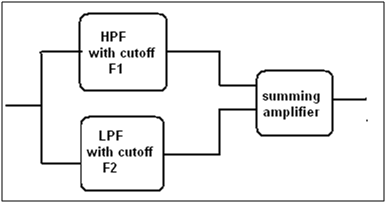
An overview of a wide band-reject filter.
2. The narrow band-pass filter: suppresses a single frequency or a few frequencies near the center frequency.
Wide band-reject filter
The wide BRF is comprised of a combination of LPF and HPF as shown above. In this case, F1 > F2. This means we have to design the HPF with F1 and LPF with F2. Let’s also suppose that we want to suppress the band of frequencies between 10 and 20 kHz. So, F1 = 20000 Hz and F1 = 10000 Hz.
Designing the HPF section
- Step 1: First assume the required value of the capacitor. It should be less than 0.1 micro Farad. This is required for better frequency stability. Let’s assume a value of C as 1 nF (nano farad).
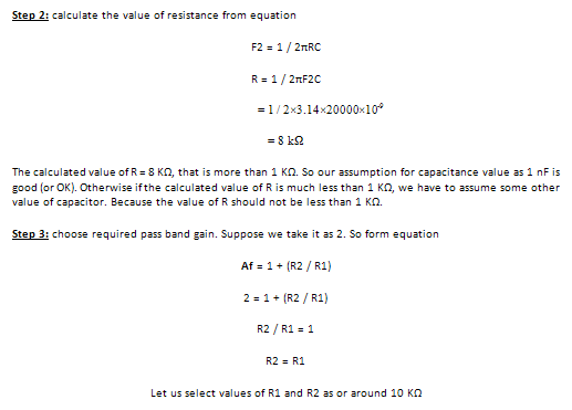
The calculations required to find the resistance and pass-band gain for the HPF section.
Designing the LPF section
- Step 4: Now, assume the required value of the capacitor. For this tutorial, we’ll assume the value C as 10 nF.

The calculations required to find the resistance and pass-band gain for the LPF section.
The final design with component values is as shown here. The op-amp is an active component and it requires +ve and -ve biasing voltages. It’s possible to test the circuit by applying an input through the signal generator and observing the output on the DSO or oscilloscope, as well as the bode plotter.
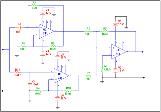
A circuit diagram of the LM741 OPAMP IC-based band-reject filter.
Note: I have simulated the above circuit in NI’s multisim 11 software. The schematic design is also prepared using the same software. The software is available as a free one-month trial period from National Instrument’s (NI) website. The below circuits are also prepared using the multisim 11 software and tested in it.
Narrow bank-reject filter (or notch filter)
- Step 1: Select the notch frequency, which is the frequency that will be rejected. These filters are typically used to remove power-line frequency that’s 50 Hz. So, take Fn = 50 Hz.
- Step 2: Assume that the capacitor value of C is 1 micro F (because the frequency is so low, the capacitor value should be large).
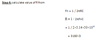
The calculations required to find the resistance of the notch filter.
- Step 5: To construct the T network with C – R/2 – C, we’ll require an R/2 value. So, simply connect the two resistors in parallel with the same R value.
- Step 6: To construct T network with R – 2C – R, we’ll require a 2C value. Now connect the two capacitors in parallel with the same C value.
Here’s the final design:
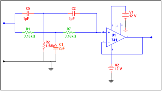
A circuit diagram of the LM741 OPAMP IC-based notch filter.
Filed Under: Tutorials


Questions related to this article?
👉Ask and discuss on EDAboard.com and Electro-Tech-Online.com forums.
Tell Us What You Think!!
You must be logged in to post a comment.