The simplest of electronic devices is a diode. It’s often referred to as a semiconductor diode but, technically, a diode has its own specific electrical characteristics. The is true for all electronic devices. They’re defined by unique electrical characteristics even though different construction, types, and applications may be available.
Having said this, a semiconductor diode is the most common and basic construction of a diode device.
Understanding diodes
As an electronic device, a diode is a two-terminal, one-way switch. In response to an applied signal, it acts as a closed switch for one-voltage polarity and an open switch for the reverse polarity.
Two important feature define an electronic device as a diode:
1. It’s a two-terminal device
2. It allows the conduction of current in one direction and opposes the conduction of current in the reverse direction.
As a result, any diode has two unique regions, regardless of its type. One is an active region, where an applied voltage polarity allows the diode to conduct current through it. The other is a reverse bias region, where an applied polarity makes the diode oppose the conduction of current.
A diode is a simple device, but it has endless applications.
The semiconductor diode
A semiconductor diode is the most basic diode construction. In fact, the concept of a diode device evolved from the semiconductor diode. All semiconductor devices are constructed by joining intrinsic semiconductor materials — p-type extrinsic and n-type extrinsic.
Both of these materials are formed on an intrinsic substrate by doping acceptor impurity atoms on the p-type and donor impurity atoms on the n-type regions, respectively. This creates a p-n junction.
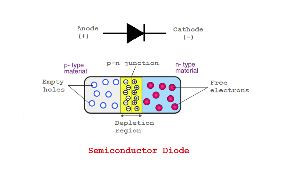
The p-n junction — with the p- and n-type materials on either side, with respective output (conducting) terminals — is a semiconductor diode.
The intrinsic material that’s subjected to doping to form the p-n junction can be silicon, germanium, or gallium arsenide.
A diode, as a simple p-n junction, represents the basic function of all semiconductor devices. The same principles that apply to a semiconductor diode apply to other sophisticated semiconductor devices, regardless of their design, complexity, operation, or characteristics.
This is why learning about a semiconductor diode is foundational to modern electronics.
Diodes at work
In a semiconductor diode’s p-type material, the holes are the majority-charged carriers and the electrons are the minority-charged carriers. In the n-type material, it’s reversed. The electrons are the majority-charged carriers and the hole are the minority-charged carriers in n-type material.
The minority carriers in both of the materials represent the contribution of the intrinsic substrate and the majority carriers represent the contribution of the impurity atoms. The concentration of the majority-charged carriers is 100,000 times greater than the minority carriers in both of the materials.
Additionally, they can both have different doping levels, which does not affect the electrical neutrality of either the materials or the diode.
As mentioned, a diode is a two-terminal device. The p-type material’s conducting end is an anode and the n-type’s conducting end is a cathode terminal.
As a result of its electrical characteristics, a diode has a couple of operating regions.
- In the active region of its voltage-current characteristics, it allows for the conduction of conventional current from its anode to its cathode.
- In the non-conducting region of its voltage-ampere characteristics, it blocks any flow of conventional current from its cathode to its anode.
As a voltage-controlled, two-terminal device, a diode has three possible electrical conditions:
1. No external voltage is applied to the diode
2. The anode is at a higher potential than the cathode
3. The cathode is at a higher potential than the anode
The electrical conditions…
No applied bias: In the absence of any external voltage across the diode, there is no current flow through it. As soon as the p- and n-type materials form a junction, the holes from the p-type diffuse in the n-type material, near the junction. This results in a layer of positive ions in the n-type material and around the junction.
Similarly, electrons from the n-type diffuse in the p-type material, near the junction. This results in a layer of negative ions in the p-type material and around the junction. This forms a depletion region at the junction, which is void of any free-charge carriers on either side.
As the majority-charged carriers are in high concentration — there are almost 100,000 times more minority carriers in both materials — only a few of the majority carriers have sufficient energy to cross the depletion region (because of the heat and light).
To cross through the diode, the holes in the p-type material will attempt to overcome the attractive force of negative ions on the p-type side of the junction and the repulsive force of the positive ions on the n-type side of the junction.
To cross through the diode, the electrons in the n-type must also overcome the attractive force of positive ions on the n-type side of the junction and the repulsive force of negative ions on the p-type side of the junction. Only a few majority carriers gain sufficient kinetic energy to cross over this depletion region, which is canceled out by the movement of the minority carriers across the junction.
As a result, in the absence of any applied voltage, there’s no current across the diode. So, the only way, current can flow through the diode is if majority charge carriers gain enough kinetic energy to cross over the junction under the influence of an external electric field.
Forward bias: When an anode is at a higher potential than a cathode, the diode is considered forward biased. Due to the positive potential at the conducting end of the p-type material, the holes in this material are pushed toward the n-type. Similarly, due to the negative potential at the conducting end of n-type material, the electrons in this type of material are pushed toward the p-type.
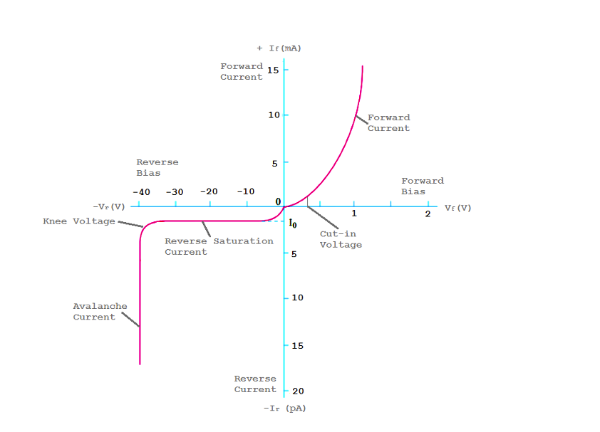
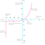
As a result, the depletion region begins decreasing. At a particular positive voltage difference, known as the cut-in voltage, the depletion region allows for an abundance of majority carriers from both sides to flow across the diode. This causes an exponential rise in the current across the diode.
As the forward bias voltage increases beyond the cut-in voltage, many majority carriers gain enough kinetic energy (under the influence of the external voltage) to cross the depletion region.
The current will continue to rise with forward-applied voltage until it reaches a maximum limit, whereby the diode acts much like a conductor. The maximum current across the diode in a forward-biased condition is limited by the concentration of the free-charge carriers in both materials. The higher the dopant level of both materials, the greater the forward current limit of the diode.
After the forward voltage is removed from the diode, the depletion region slowly recovers and the diode returns to a non-conduction state, as is the case without any applied voltage.
Reverse bias: When a cathode is at a higher potential than an anode, the diode is considered to be in reverse bias. The negative potential at the conducting end of the p-type material pulls the holes of this material toward its conducting end. Likewise, the positive potential at the conducting end of the n-type pulls the electrons of this material towards its conducting end.
As a result, the depletion region widens and the majority-charged carriers in both materials have no chance to cross the depletion region. To cross the diode, this voltage polarity lets the minority carriers contribute via the intrinsic substrate on both sides. An extremely small current (due to the minority carriers), known as reverse saturation current,
flows through the diode. This is called a reverse saturation current because it quickly reaches a maximum limit, beyond which, it will not change.
The reverse saturation current is typically represented in nano amperes or microamperes, except in high-power diodes. The actual reverse current is greater than the reverse saturation current as it includes other factors such as leakage currents, temperature sensitivity, junction area, and charge carriers in the depletion region.
In the electronic circuits, this is such a small amount of current that it’s negligible compared to the current in the conducting wire and other current-active components of a network.
Breakdown region: In a reverse bias condition, the depletion region widens as the reverse voltage increases. Because of the high reverse voltage, at a certain point, the minority carriers gain enough kinetic energy that they initiate a process of ionization by colliding with the atoms. As a result of ionization, several carriers are released in both materials that are capable of crossing through the diode. This causes a high avalanche current to flow from the cathode to the anode.
The heavy breakdown of minority carriers is referred to as an avalanche breakdown. The maximum reverse voltage before a heavy avalanche current is triggered across the diode is called a peak reverse voltage (PRV), a peak inverse voltage (PIV), or a knee voltage.
The characteristics region beyond the PIV rating is the Zener region. By increasing the dopant level of the p- and n-type materials, the PIV rating can be brought closer to -5V. Due to an increased doping level, another phenomenon, known as Zener breakdown, occurs in which the increased current level is due to the strong electric fields disrupting the atomic bonds in the doped materials.
A special semiconductor diode heavily doped to have a Zener Breakdown in reverse bias condition is a Zener diode. Zener diodes are used for voltage regulation.
Voltage-current characteristics
A diode has two operating regions. In a “no bias” condition, there’s zero current flowing through it. In a forward bias, the diode goes into a conduction state. This means it allows a small current to pass through the anode until the cut-in voltage is reached.
Beyond the cut-in voltage, the current rises exponentially as per the equation:
I = Is*eVD/nVT – Is
Where…
- I is the current through the diode
- Is is the reverse saturation current
- VD is the applied forward bias voltage
- n is the ideal factor, which ranges between one and two, depending on the operating conditions and the construction of the diode
- VT is thermal voltage
The thermal voltage is:
VT = k*TK/q
Where…
- VT is the thermal voltage
- k is the Boltzmann’s constant = 1.38*10-23 J/K
- TK is the absolute temperature in Kelvin
- q is charge of electron = 1.6*10-19 C
In forward bias, the forward current through the diode increases exponentially with the forward-bias voltage. The value of thermal voltage also increases with the temperature. Therefore, as the temperature rises, the forward current decreases, and as the temperature decreases, the forward current increases.
In reverse bias, the reverse saturation current due to minority carriers is the only current that flows through the diode until the knee voltage is reached. The forward current is in the range of mA and rises by the tenths of volts of the forward bias. The reverse bias voltage is in the tens of volts and the reverse saturation current is typically in the pA or uA.
The cut-in voltage, reverse saturation current, and knee voltage are dependent on the minority-charged carriers, which are contributed by the intrinsic substrate. Therefore, the cut-in voltage, reverse saturation current, and knee voltage are dependent on the substrate material.
The cut-in voltage for:
- Silicon (Si) diodes: 0.7V
- Germanium (Ge) diodes: 0.3V
- Gallium arsenide (GaAs) diodes: 1.2V
The reverse saturation current for:
- Silicon (Si) diodes: 10pA
- Germanium (Ge) diodes: 1uA
- Gallium arsenide (GaAs) diodes: 1pA
The peak inverse voltage of:
- Silicon (Si) diodes: 50V~1kV
- Germanium (Ge) diodes: 100-400V
- Gallium arsenide (GaAs) diodes: 100V~20KV
DC signal response
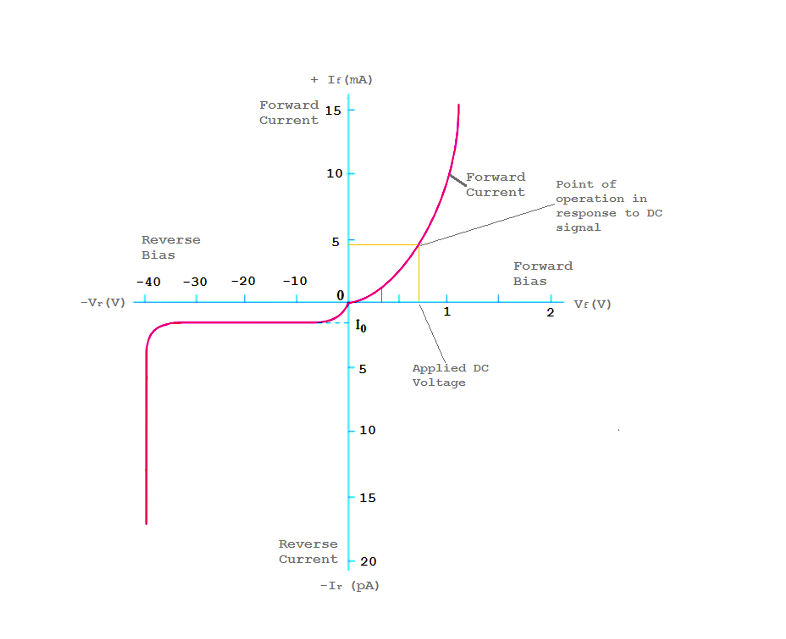
When a DC signal is applied to a diode, it operates at a specific point related to its characteristic curve. The current flows through the diode only when the DC signal is applied in a positive polarity.
According to the point of operation, the diode conducts a fixed, forward current in an mA range, offering a fixed DC/static resistance.
AC response
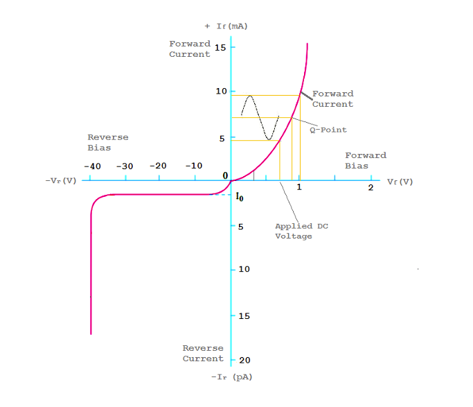
When an AC signal is applied to a diode, its point of operation on the characteristic curve continuously changes between the positive and negative peaks of the applied signal.
The current through the diode passes up and down a quiescent point or Q-point. This Q-point is useful for determining the instantaneous AC resistance of the diode to the signal. The instantaneous AC resistance is derived by the tangent at the Q-point of the operating signal. The average AC resistance is determined by the change of voltage to the change in current over the positive and negative peaks of the AC signal.
If the applied signal has lower peak voltage levels, the AC resistance from the diode to the signal is higher. If the applied signal has greater peak voltage levels, the AC resistance from the diode is smaller.
Electrical characteristics
A few important electrical characteristics of a semiconductor diode are:
- Cut-in voltage
- Maximum forward current
- Reverse saturation current
- Reverse current
- PIV rating
- Zener voltage
- DC resistance
- AC resistance
- Average AC resistance
- Transition capacitance
- Diffusion capacitance
Types of diodes
The semiconductor diode is not the only type of diode available. However, there are several types of semiconductor diodes, each designed to operate within specific characteristic regions or to offer specific physical or electrical properties.
A few examples include power, Zeners, small-signal, large-signal, light-emitting diodes, and others.
For example, there are many diodes with special constructions such as laser, Shockley, and Shottky diodes, etc. Regardless of the construction, operating features, or physical properties, the characteristic curve and electrical behavior of all diodes remain similar.
All diodes are voltage-controlled, two-terminal, one-way switches.
You may also like:
Filed Under: Tech Articles



Questions related to this article?
👉Ask and discuss on Electro-Tech-Online.com and EDAboard.com forums.
Tell Us What You Think!!
You must be logged in to post a comment.