Most of the electronic devices work on a single positive power supply except few like op-amps, oscillators etc. Majority of the amplifiers circuits or amplifiers ICs are also works on positive power supply. Such kind of devices can operate only with input signals having only positive voltages. Devices like amplifiers, modulators, demodulators etc. are supposed to work with natural signals as input. Since the natural signals like sine wave, audio signals etc. has both positive and negative cycles they have to be modified in such a way the single supply electronic circuits can operate them.
Clamping is the common technique that is applied on the input signals to modify them so that the circuits can process the entire signal without losing either positive or negative half. In this method the entire waveform is shifted to positive of negative voltage side hence making them single polarity varying voltage. This article discusses the details of the clamping and the practical positive and negative clamping circuits.
DESCRIPTION:
The waveforms having both positive and negative half cycles can be clamped to either positive or negative voltage side. When the entire waveform is shifted to the positive side it is called positive clamping of a waveform. The negative clamping is the method in which the entire waveform is shifted to the negative voltage side.
The following represents the clamping of a sine wave using both the positive and negative clamping devices.


Fig. 1: Clamping of Sine Wave using both Positive and Negative Clamping Devices
The positive or negative clamping of a sine wave can be achieved by using a single diode and a capacitor. Here the positive and negative clamping of a sine wave is demonstrated with the help of a Wien Bridge oscillator circuit which can generate a sine wave. The Wien Bridge is a circuit which can generate the pure sine wave with minimum distortion.
The circuit used here to generate the sine wave based on Wien Bridge has both the frequency and amplitude adjustments. The circuit diagram of the variable frequency sine wave oscillator is shown in the following:
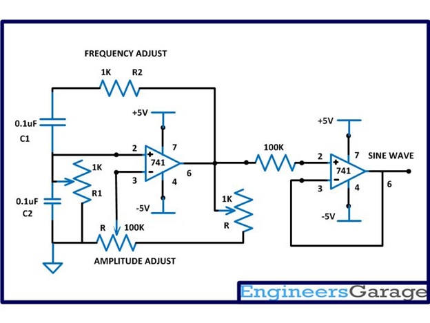
Fig. 2: Circuit Diagram of Variable Frequency Sine Wave Oscillator
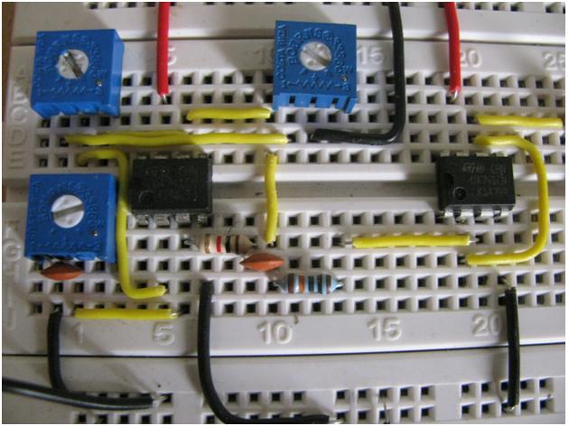
Fig. 3: Circuit of Variable Frequency Sine Wave Oscillator on Breadboard
The frequency of the above circuit can be varied by simply varying the potentiometer R2 and the amplitude of the wave form can be adjusted by varying the potentiometer R. The frequency of the sine wave generated by the above circuit depends on the components R1, R2, C1 and C2 and the equation for the frequency is given below:
For the ease of adjusting the amplitude of the wave to obtain proper sinusoidal sweep, a coarse and fine adjustment has been implemented using potentiometers. A low value (1K) potentiometer is connected in series with the high value (100K) potentiometer so that the coarse adjustment can be done with the high value resistor and the fine adjustment with the low value resistor.
POSITIVE CLAMPING
The clamping circuit requires only a diode and a capacitor and in the case of positive clamping the positive end of the diode is grounded and the wave is received at the other end through a capacitor. The circuit of the positive clamper is shown below:

Fig. 4: Circuit Diagram of Positive Clamper
The above circuit forms the simplest positive waveform clamper, but it cannot be directly used in most of the circuits since it cannot be loaded. When a load of very small resistance is applied at the output end of the circuit it may not work properly. Hence a buffer (current amplifier) must be added at the output end of the circuit as shown in the following diagram
Positive Clamping
The diode 1N4148 is used in the circuit since it can be operated in very high frequencies and also the bias voltage is as low as 0.3 V. The capacitor of value 0.1uF is a capacitor without any polarity and commonly used in coupling audio frequency waves.
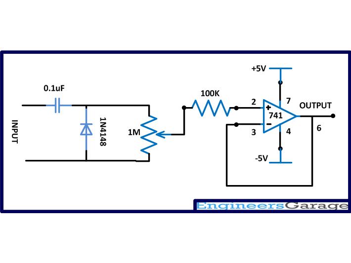
Fig. 5: Circuit Diagram of Positive Clamper with Buffer
The 1M ohms is a potentiometer that can be used to adjust the amplitude of the clamped wave that can be applied to the current amplifier without loading the clamping circuit itself. A 100K ohms resistor is also used at the input side of the current amplifier circuit which will prevent the loading of the clamping circuit by the input resistance of the current amplifier circuit.
The image of the circuit wired in the breadboard is given in the following:
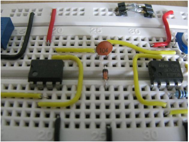
Fig. 6: Positive Clamping Circuit on Breadboard
The input of the clamper circuit with the current amplifier can be provided with a pure sine wave input from the previous sine wave generator circuit. The following circuit diagram shows the combined circuit made by connecting the sine wave generator and the positive clamping circuit together.

Fig. 7: Circuit Diagram of Sine Wave Generator and Positive Clamping
The variable frequency sine wave generator adjusted in such a way that it will generate a pure sine wave of 1 KHz. The input and output waveforms of the above circuit observed in CRO are given in the following figures:
The input waveform:
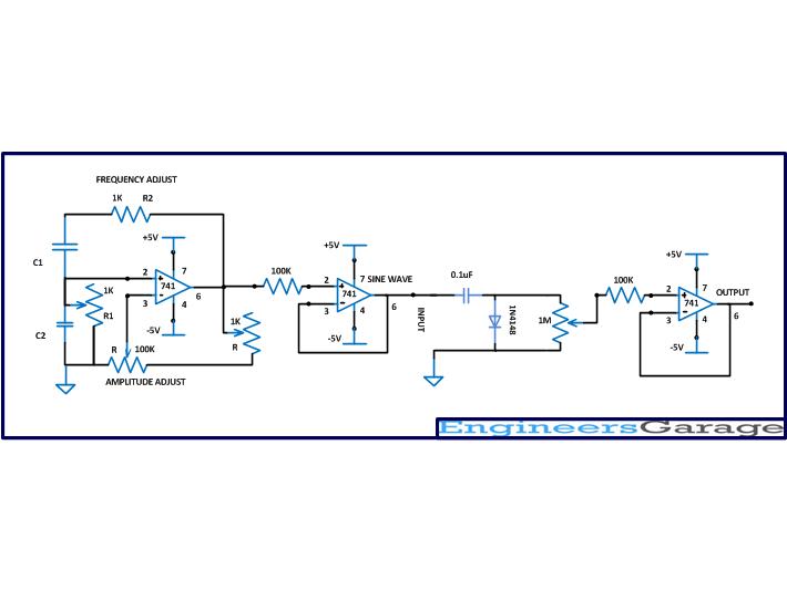
Fig. 8: Positive Clamper Input Waveform on CRO Screen
The positive clamped output waveform:

Fig. 9: Positive Clamper Output Waveform on CRO Screen
It can be noticed from the above image is that a small portion of the clamped waveform is still beneath the 0 voltage. The amplitude of the waveform below the 0 voltage will be exactly equal to the bias voltage of the diode used and in this case since the 1N4148 is used the amplitude of waveform in the negative side will be 03V.
Negative Clamping
NEGATIVE CLAMPING
The clamping circuit requires only a diode and a capacitor and in the case of negative clamping the negative end of the diode is grounded and the wave is received at the other end through a capacitor. The circuit of the negative clamper is shown below:

Fig. 10: Circuit Diagram of Negative Clamper
The above circuit forms the simplest negative waveform clamper, but it cannot be directly used in most of the circuits since it cannot be loaded. When a load of very small resistance is applied at the output end of the circuit it may not work properly. Hence a buffer (current amplifier) must be added at the output end of the circuit.
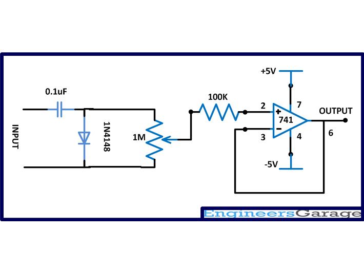
Fig. 11: Circuit Diagram of Negative Waveform Clamper with Buffer
The image of the circuit wired in the breadboard is given in the following:

Fig. 12: Negative Clamping Circuit on Breadboard
The input of the clamper circuit with the current amplifier can be provided with a pure sine wave input from the previous sine wave generator circuit. The following circuit diagram shows the combined circuit made by connecting the sine wave generator and the positive clamping circuit together.

Fig. 13: Circuit Diagram of Sine Wave Generator and Negative Clamping
The variable frequency sine wave generator adjusted in such a way that it will generate a pure sine wave of 1 KHz. The input and output waveforms of the above circuit observed in CRO are given in the following figures:
The input waveform:
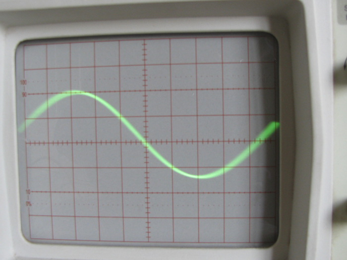
Fig. 14: Negative Clamper Input Waveform on CRO Screen
The negative clamped output waveform:
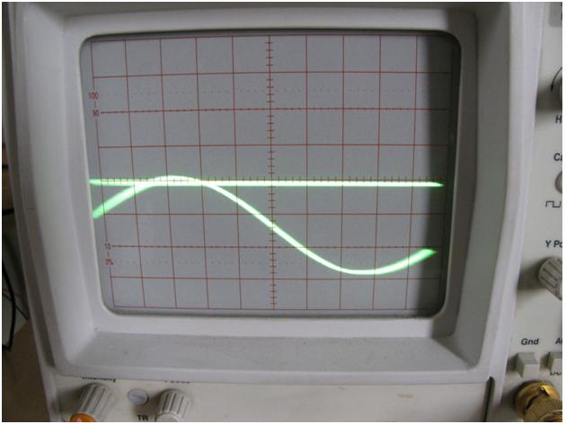
Fig. 15: Negative Clamper Output Waveform on CRO Screen
It can be noticed from the above image is that a small portion of the clamped waveform is still above the 0 voltage. The amplitude of the waveform above the 0 voltage will be exactly equal to the bias voltage of the diode used and in this case since the 1N4148 is used the amplitude of waveform in the negative side will be 03V.
Filed Under: Circuit Design


Questions related to this article?
👉Ask and discuss on EDAboard.com and Electro-Tech-Online.com forums.
Tell Us What You Think!!
You must be logged in to post a comment.