Electronic number game circuit is an interesting game for children and elders or you can play with your friends. In this you have to perform mathematical operation like addition, subtraction, multiplication, division and in the end the person who has the highest score will win the game.
So you can also play this game with your children and teach them the mathematical operation very easily and interestingly.
There is no limit on the number of person who can play this game.
Important feature of this circuit is it will display the number on 7 segment display so you can easily see the number on display easily. And it will hold the display until you have hold the touch to stop wire.
[[wysiwyg_imageupload:10874:]]
Fig. 1: Prototype of Electronic Number Circuit on Breadborad
Assemble the circuit properly and apply power supply. You will see random number are generating on 7 segment display and all mathematical operation performing LED’s are also glowing randomly. Now hold the touch to stop point in your hand random number will be display on 7 segment display and one LED will also like 7 with minus LED, but for the first time we will take the number that is 7 and ignore the LED. This is our first number. Again leave the touch to stop wire now all LED’s and display will give you random number then again hold the touch to stop switch than another number and LED will glow like in our example 6 with subtraction sign. Now again do the same process we will get
7-6-0-2+8*9 = 63 as your score. Now compare this with person who are playing with you and the person who has the highest score will be declare as winner.
This circuit is based on 3 IC namely NE555, CD4017 and CD4033 and 7 segment common cathode displays with few more components.
In this circuit NE555 is used to generate the clock pulse which is provided to CD4017 and LED to indicate which mathematical operation to be performed and CD4033 is used to display number on 7 segment display respectively. And CD4017 is a CMOS counter/ divider IC. It take clock signal from the clock input and turn on the 10 output in sequence, each time when it receives clock input pulses.
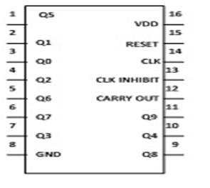
In order to understand the working of IC one must know about its individual pin. It has 3 input pin and 10 output pin and one is ground pin and another is used for power supply and one is Carry out pin. Pin diagram of CD4017 is Shown below-

Fig. 2: Pin Diagram of CD4017
1. Input pin–
a. Reset pin (pin 15) – It is used to reset the counter to zero. Like you want the counter to count up to third output then connect the fourth output to pin 15. Now after every third output it will automatically starts counting from zero.
b. Clock pin (pin14)- Whenever pin 14 goes high it will provide you the output. Like for first clock pulse pin 3 will provide you output similarly for next pulse pin 2 will provide output and so on. After 10 pulse it will again start from Q0 output.
c. Clock Inhibit pin (pin 13)- It is used to switch the counter “on” and “off”. When you want to switch off the counter then pin 13 should be high. If it is high it will ignore the clock pulse no matter how many times you press the switch means the count will not advance. In our circuit we have ground the pin 13.
2. Output pin (pin Q0- Q9)- It is used to receive the output in sequential manner. Like for first pulse pin 3 will provide you the output and so on.
3. Ground pin (pin 8) and Supply pin (pin 16)- It is used to provide ground and power supply to the IC for its working.
4. Carry out pin (pin 12)- It is used to connect one or more CD4017 IC’s. Like if you want to add one more CD4017 IC then connect Pin 12 to Clock input of its successor. The carry pin of first CD4017 is connected to clock input of second and the carry pin of second is connected to the clock input of third and so on. In our circuit we have used only one IC that’s why we have left this pin.
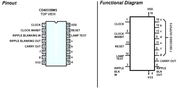
And CD4033 is a Johnson counter IC commonly used in digital display. It has a 5 stage Johnson decade counter with decoder which convert the Johnson code to a 7 segment decoded output. Means it will convert the input into numeric display which can be seen on segment display or with the help of LED’s. To understand its working first have a look on its
pin diagram –

Fig. 3: Pin Diagram and Functional Diagram of CD4033
Now let us understand the working of individual pins-
1. Pin 1 known as Clock in – It receives clock signals, and at every positive clock counter advances one by one. You can provide clock with the switch, 555 timer or with the help of logic gates.
2. Pin 2 known as Clock inhibit – CD4033 counter advances one by one by receiving positive pulse at this time clock inhibit pin should be grounded. If it is connected to supply than counter advancement will be inhibited means there will be no meaning of clock pulse.
3. Pin 3 and pin 4 known as Ripple blanking in and Ripple blanking – It is used to display only one zero blanking the other zero. For this IC have ripple blanking in and ripple blanking out. For example you want to display 345 and you are using five 7 segment display then it will display 00345 if blanking input and out is off. But if it is on than you will receive 345. It improves the readability of the circuit.
4. Pin 5 known as carry out – It is used to complete one cycle for every 10 clock input cycle and it also used to cascade more IC’s.
5. Pin 6, pin7 and Pin9 to pin 13 – These are 7 decoded output from a to g used to illuminates the corresponding segment of 7 segment display to display the digit from 0 to 9.
6. Pin 14 known as Lamp test – It is used to check that all segments of 7 segment is working properly or not. For testing momentarily make the pin low.
7. Pin 15 known as Reset – It is used to reset the counter. When it receives high it clears the counter and counting again starts from zero. One important thing reset pin should again made low to start the counter once again.
8. Pin 8 known as ground pin and Pin 16 known as Vdd it should be connected to power supply.
Working of circuit
In this circuit NE555 timer is continuously generating clock pulse which is given to decade counter IC2 which starts its counting and give you the outputs from Q0 to Q3 and similar pulse is also feed to Johnson counter IC3 therefore the IC will generate random number. You can vary the speed of the display and LED by varying the value of resistor R1 and Capacitor C1. Now when you press the stop switch only one LED will glow with one particular sign. You can also use push to on switch instead of touch to stop wire. CD4017 gives you 10 output but in this circuit we are utilizing only 4 that’s why we have connected the pin 10 of IC2 to pin 15 of IC2 for resetting the circuit. You can use more out puts for different mathematical operation like power, exponential etc to increase the complexity of game.
Circuit Diagrams
Project Components
Project Video
Filed Under: Electronic Projects
Filed Under: Electronic Projects


Questions related to this article?
👉Ask and discuss on EDAboard.com and Electro-Tech-Online.com forums.
Tell Us What You Think!!
You must be logged in to post a comment.