For the people who are doing PCB designing, hobbyist or professionals, there are so many PCB designer softwares available. Most popular among them are diptrace, orcad, eagle, kicad etc. This tutorial is mainly for those people who haven’t tried out any professional pcb designer software yet.
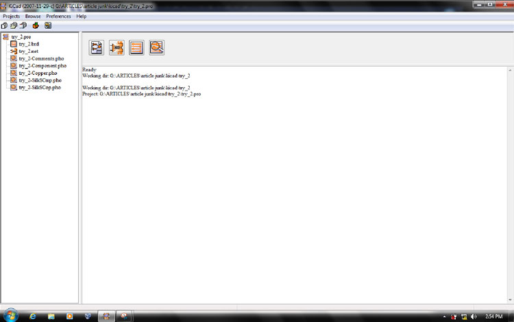
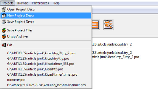
Fig. 2: Screenshot of Project Menu in KIcad

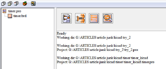
Fig. 3: Screenshot of Naming New Project in KIcad
Editing the Schematic
![]()
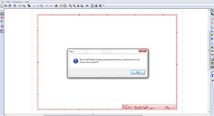
Fig. 5: Screenshot showing Eeschema Icon in KIcad
![]()
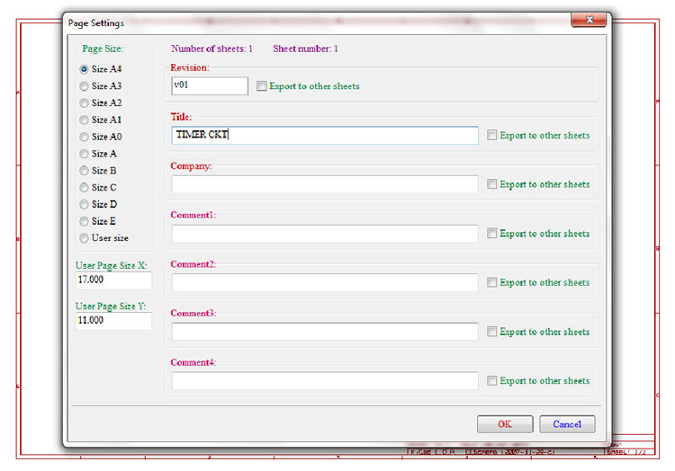

Fig. 9: Screenshot of the PCB Title in KIcad
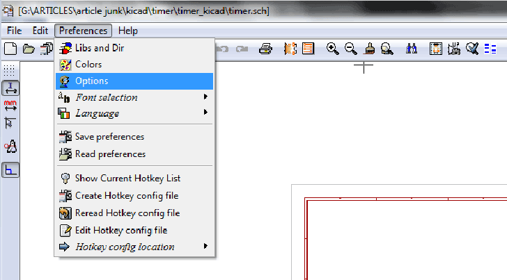
Fig. 10: Screenshot of Preferences Menu in KIcad
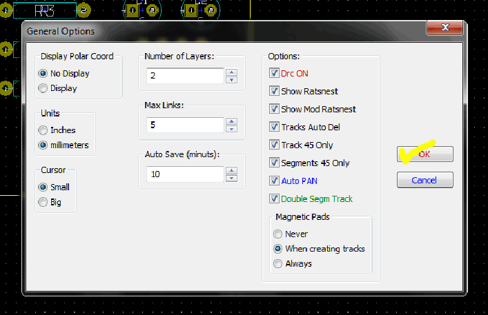
Fig. 11: Screenshot of General Options Window in KIcad
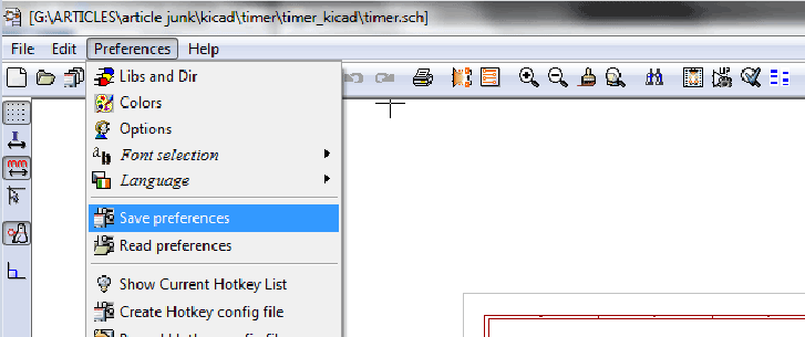
Fig. 12: Screenshot of Save Preferences in Preferences Menu of Kicad

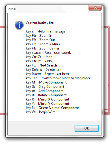
Fig. 14: Screenshot of Current Hotkey List in KIcad
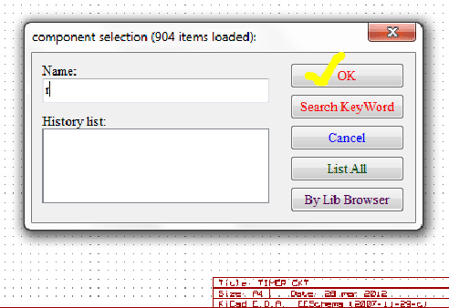
Fig. 15: Screenshot of Component Selection Window in KIcad
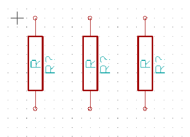
Fig. 16: Screenshot of Components Drawn in KIcad
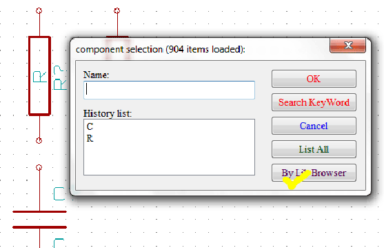
Fig. 17: Screenshot of Naming a Component in KIcad
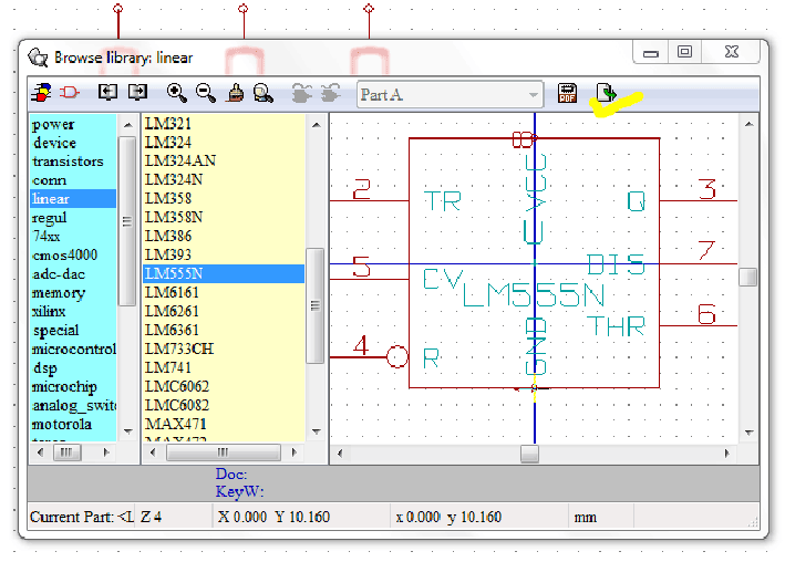
Fig. 18: Screenshot of Browsing a Component in KIcad
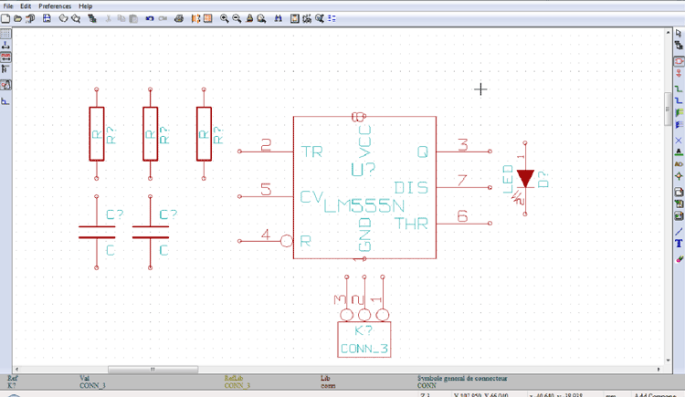
Fig. 19: Screenshot of Adding a Component in the Circuit Diagram in KIcad
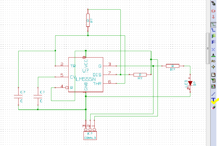
Fig. 20: Screenshot of Connecting Components in KIcad
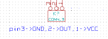
Fig. 21: Screenshot of Labeling Components in KIcad
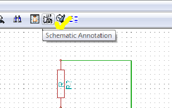
Fig. 22: Screenshot of Schematic Annotation Button in KIcad
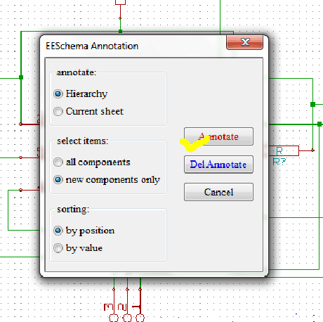
Fig. 23: Screenshot of EESchema Annotation Window in KIcad
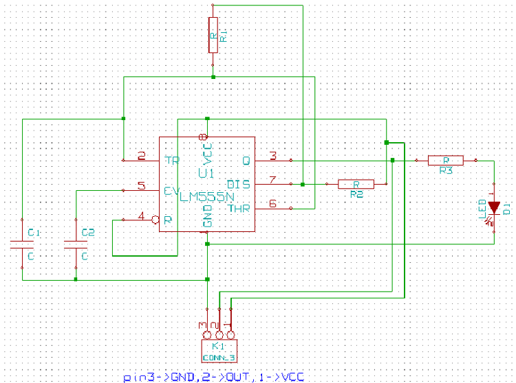
Fig. 24: Screenshot of Final Circuit Designed on KIcad

Fig. 25: Screenshot of ERC (Electric Rules Check) Button on KIcad
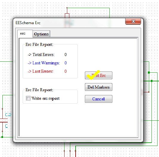
Fig. 26: Screenshot of EESchema Erc Window in KIcad
If there are errors, which mean you have violated some rules. The errors will be shown in the schematic using markers and you can easily identify and correct those errors. If you have no idea about the ERC, don’t worry, it is not going to affect most of the simple circuits in anyway.
 .
.
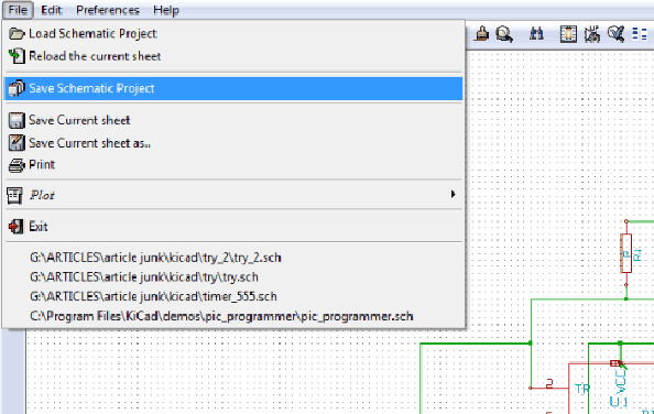
Fig. 27: Screenshot of File Menu in KIcad
2) Components to modules
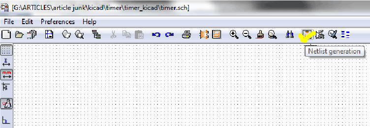
Fig. 28: Screenshot of Netlist Generation Button in KIcad

Fig. 29: Screenshot of Read Netlist Button in KIcad
Save the netlist file using the extension .net:

Fig. 30: Screenshot of Naming Netlist file in KIcad
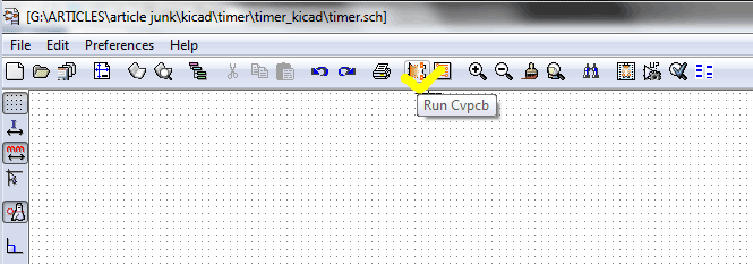
Fig. 31: Screenshot of Run Cvpcb Button in KIcad
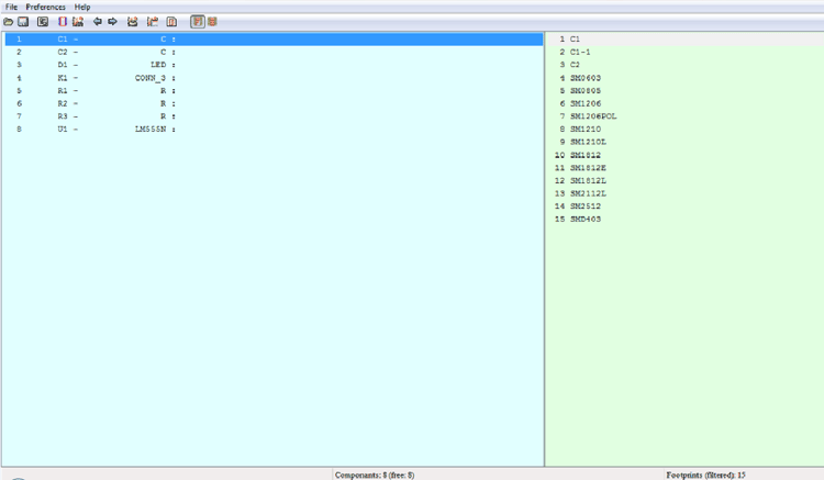
Fig. 32: Screenshot of Cvpcb Window in KIcad
For each component listed we must select the required footprint. It would be better if you list the entire footprint without filtering:
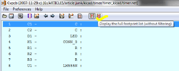
Fig. 33: Screenshot of Display the Full Footprint List Button in KIcad
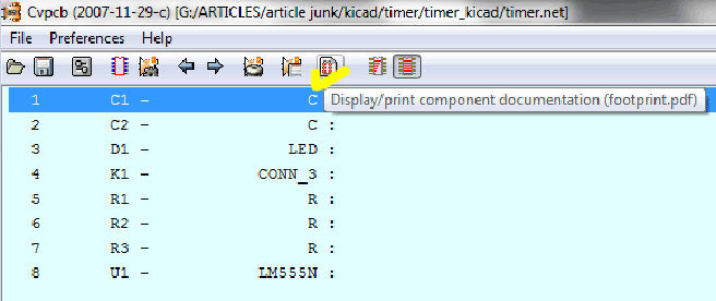
Fig. 34: Screenshot of Display Component Documentation Button in KIcad
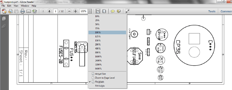
Fig. 35: Screenshot of Zoom Button in KIcad
I’ve a couple of small electrolytic capacitor for the circuit which matches the following footprint like:

Fig. 36: Screenshot of Capacitor Footprint in KIcad
If you want to see the selected footprint in detail, keep the footprint selected in the list and press view selected part:
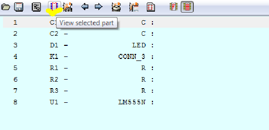
Fig. 37: Screenshot of View Selected Part Button in KIcad
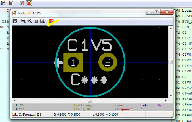
Fig. 38: Screenshot of a Footprint in KIcad
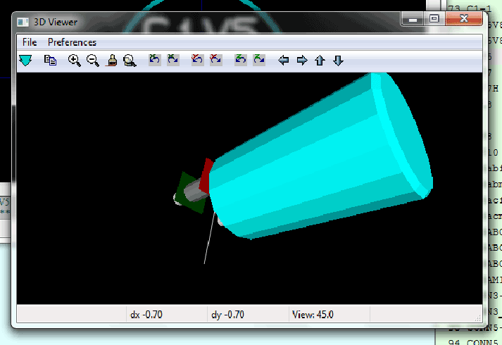
Fig. 39: Screenshot of 3D View in KIcad
Close both the windows and double click the required footprint to get it selected. If you finish selecting the footprints, the page will look like the following:

Fig. 40: Screenshot of Saving Netlist Button in Kicad

Fig. 41: Screenshot of Saving Netlist in KIcad
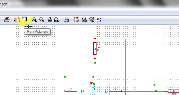
Fig. 42: Screenshot of Run Pcbnew Button in KIcad
PCB Editing
3) PCB Editing
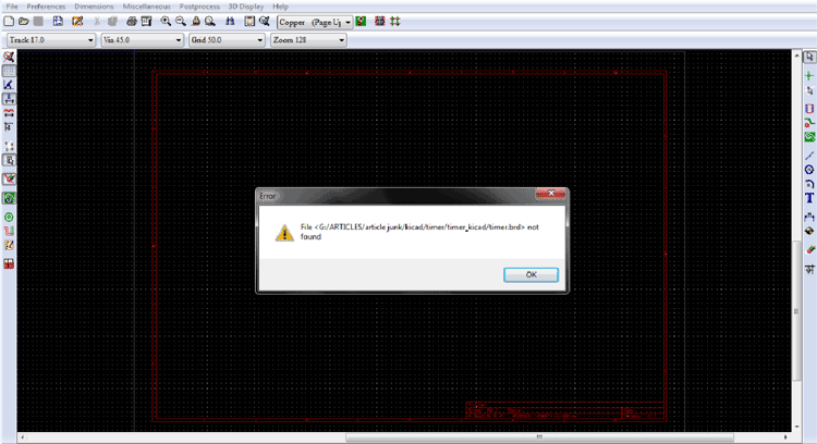
Fig. 43: Screenshot of PCBnew Window in KIcad
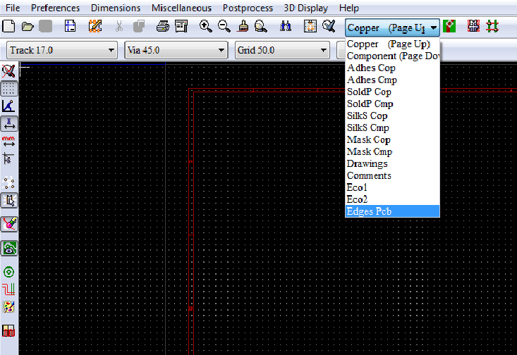
Fig. 44: Screenshot of Layer Menu in PCBnew in KIcad
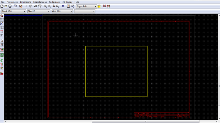

Fig. : Screenshot of Read Netlist Button in KIcad
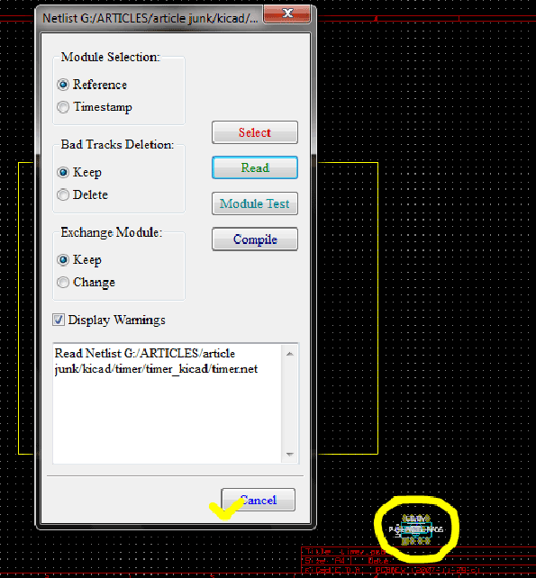
Fig. 46: Screenshot of Netlist Window in KIcad

Fig. 47: Screenshot of Netlist Window in KIcad
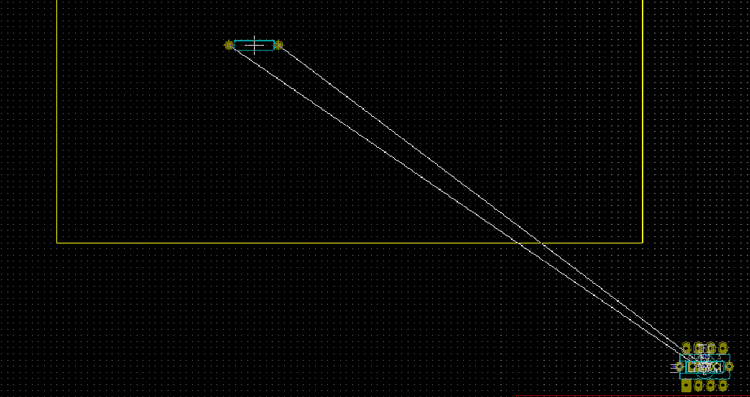
Fig. 48: Screenshot of Arranging Components on Layout in KIcad
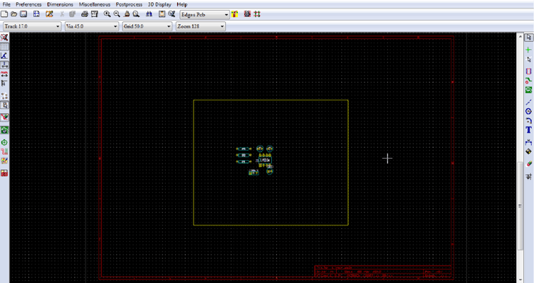
Fig. 49: Screenshot of Rearranged Components in KIcad
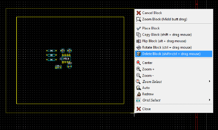
Fig. 50: Screenshot of Option Delete Block in KIcad
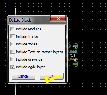
Fig. 51: Screenshot of Delete Block Window in KIcad
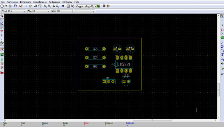
Fig. 52: Screenshot of PCB Layout After Deleting Block

Fig. 53: Screenshot of 3D Display Menu in KIcad
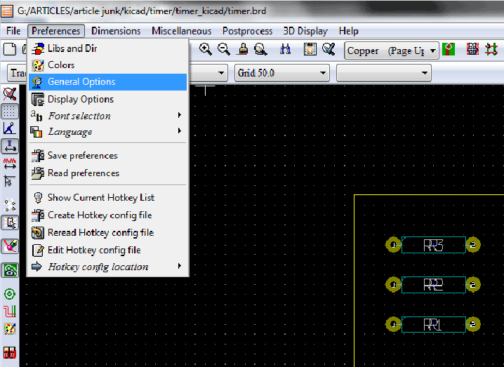
Fig. 54: Screenshot of General Options in Preferences Menu in KIcad

Fig. 55: Screenshot of General Options Window in KIcad
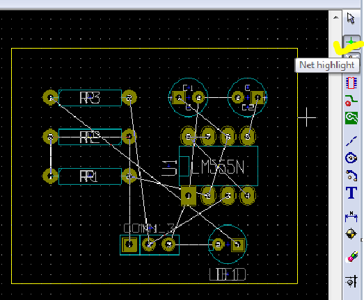
Fig. 56: Screenshot of PCB Layout in KIcad
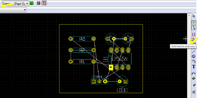
Fig. 57: Screenshot of Copper Layer in KIcad
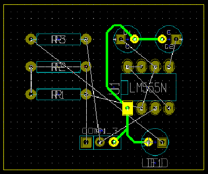
Fig. 58: Screenshot of Making Tracks on PCB Layout in KIcad
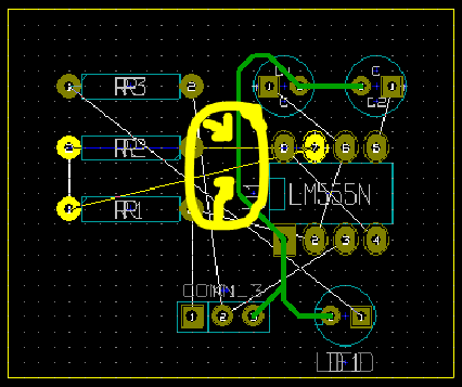
Fig. 59: Screenshot showing Trouble in Connecting Two Components on PCB Layout
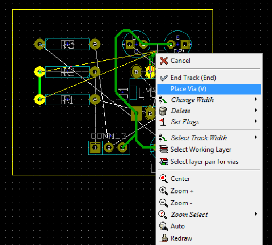
Fig. 60: Screenshot of Placing Via in PCB Layout in KIcad
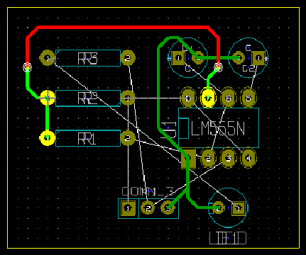
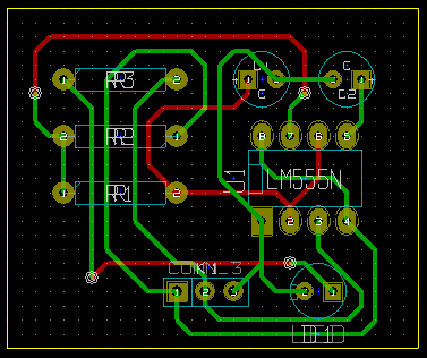
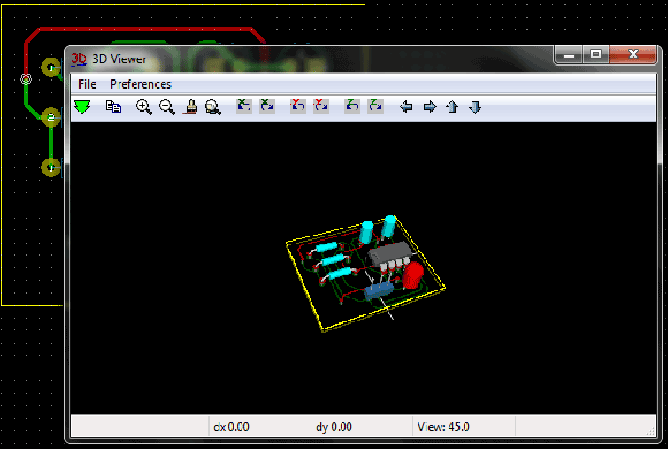
4) Generating Gerber file
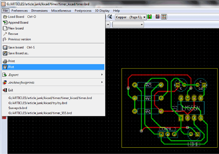
Fig. 64: Screenshot of Plot Button in File Menu in KIcad
Do the things in the plot window as shown in the following figure:
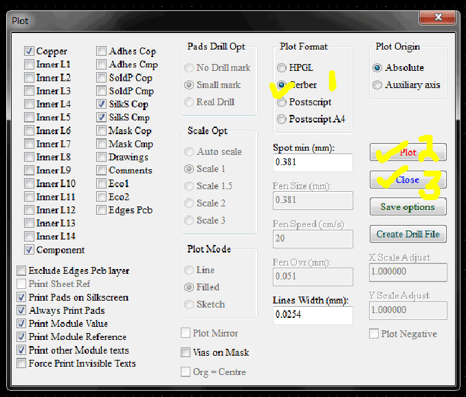
Fig. 65: Screenshot of Plot Window in KIcad

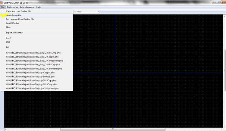
Fig. 67: Screenshot of Load Gerber File Button in File Menu of KIcad
Let us view the copper layer first.
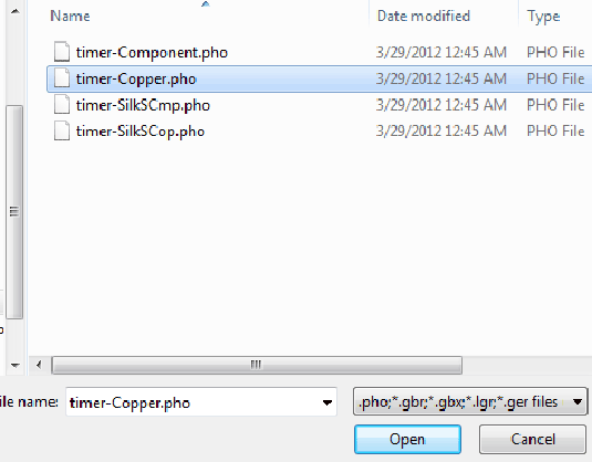
Fig. 68: Screenshot of Copper Layer File
Gerber view for the copper layer:

Fig. 69: Screenshot of Copper Layer File
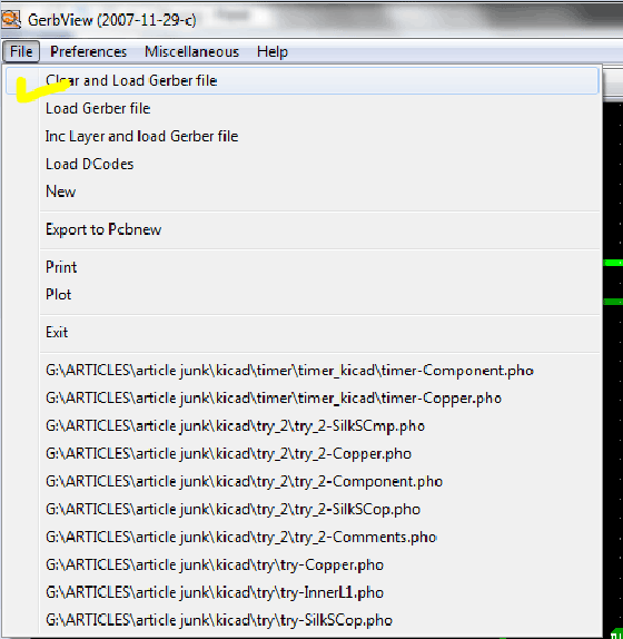
Fig. 70: Screenshot of Gerber View for the Copper Layer
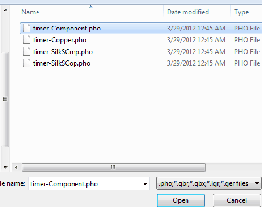
Fig. 71: Screenshot of Component Layer File
The Gerber view of component layer will look like this:

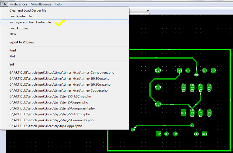
Fig. 73: Screenshot of Inc Layer and Load Gerber File Button in File Menu of KIcad
Gerber view of the selected layers will look like the following:
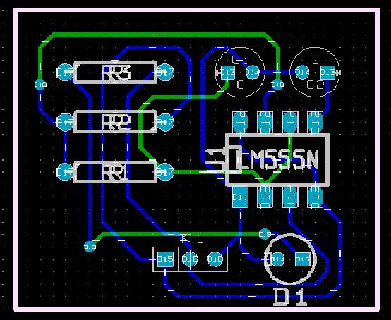
Fig. 74: Screenshot of Gerber View of the Selected Layers in KIcad
Now you select the option “Save set up”.
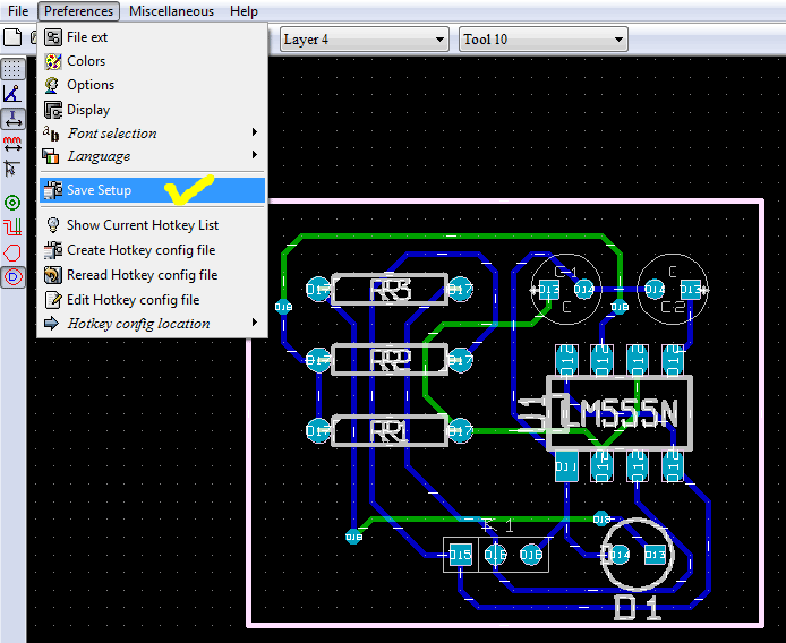
Fig. 75: Screenshot of Save Set up Button in File Menu in KIcad

Fig. 76: Screenshot of Saving the Gerview File as the extension .cnf
Filed Under: Tutorials


Questions related to this article?
👉Ask and discuss on EDAboard.com and Electro-Tech-Online.com forums.
Tell Us What You Think!!
You must be logged in to post a comment.