The Phase Locked Loop or PLL is a feedback system used in high quality stereo decoders, Frequency shift keying, telemetry applications, wide band FM discriminators, frequency multiplication applications etc. PLL integrated circuits are now available to minimize the component count. This note will give the working principle of PLL integrated circuits.
1. Voltage Controlled Oscillator or VCO
It is a free running Multivibrator whose Centre Frequency is determined by the external timing resistor and capacitor. By applying appropriate DC voltage, it is possible to shift the frequency to the either sides. The shift in change is directly proportional to the DC voltage applied and hence the name Voltage Controlled Oscillator. The output of VCO is an exact replica of input signal frequency minus noise.
2. Phase Comparator
The VCO output is received by a phase sensitive detector where the phase of VCO is compared with the incoming signal. The Phase comparator then gives an output whose magnitude is directly proportional to the phase difference compared. This is known as the ‘Error Signal’.
3. Low pass filter
The Output from the Phase comparator passes into a Low pass filter to remove the components of VCO and Input signal. Working of Low pass filter is an important factor to achieve “Phase Locked Loop”. If the VCO is too far away, beat frequency will be high to pass through the filter and PLL will not respond. In this case, the Signal is said to be out of the Capture Band. Once the Lock establishes, the filter never restricts the PLL. The filter limit the speed at which the PLL can track. But if the frequency changes too rapidly, the PLL becomes Unlocked. The low pass filter thus restricts the capture band and reduces the tracking speed. The charge on the filter capacitor gives a short ‘Memory’ so that even if the signal drops, the DC voltage in the capacitor will continue to shift VCO at the same rate till it accepts the input signal.
4. Error correction Amplifier
The output from the low pass filter is amplified by the Error correction amplifier. The DC from the error correction amplifier is then fed back to the VCO to complete the ‘Loop’. The feed back system shifts the VCO frequency close to the frequency of the incoming signal so that the error signal becomes negligible. Now the Signal is in the “Capture Range”.
Phase Locking
After the system achieves the Capture ranges, the VCO continues to change its frequency so as to give an output exactly the same as the input signal frequency. If it happens the system is said to be “Locked”. After the locking, if the input signals frequency changes, the VCO follows the change exactly. Thus the Phase Locked Loop has three states namely Free running, Capture and Locked.
Signal capturing
When the PLL enters into the capture state, a small sine wave appears. This sine wave is called “Beat frequency” which is the frequency between the VCO and the input signal. The DC component of the Beat frequency drives the VCO towards the Lock. Each successive cycle directs the VCO move closer to the input signal frequency and finally the VCO locks. The beat frequency then disappears.
The block diagram of PLL IC 565 is shown below.
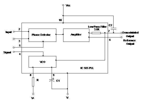
Important Features of IC 565 and 567
The important features of IC 565 are
1. Stable centre frequency at 200 ppm
2. 5-12 volt operating voltage range
3. Centre frequency can be programmed through external resistor or capacitor.
4. TTL compatible output
The VCO frequency can be calculated using the formula
F0 = 1.2 / 4 R x C1 = Hz.
IC LM 567
This PLL IC has more features than the typical 565 PLL. When the VCO lock up, the IC 567 has a circuitry to give an indication of the locking. It has an out put transistor with open collector which can be used to drive an LED or a relay to indicate the Phase Lock.

A typical Tone Decoder circuit using PLL IC LM567 is shown below
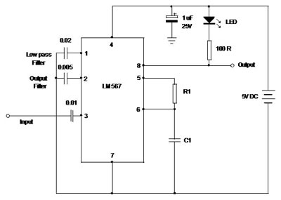
Select R1 and C1 for the desired centre frequency
F0 = 1.1 / R1 x C1
The Bandwidth of the decoder depends on the value of low pass filter and the input signal amplitude. The formula for calculating the Band width is
Band width = 1070 x Vi / f0 x C2 (0.02)
Where Vi is the input voltage in mV and C2 is the value of low pass filter capacitor in uF.
Value of Output filter capacitor C3 (0.005) should not be too high or low. It should be two times higher than that of the low pass filter capacitor.
Filed Under: Electronic Projects

Questions related to this article?
👉Ask and discuss on EDAboard.com and Electro-Tech-Online.com forums.
Tell Us What You Think!!
You must be logged in to post a comment.